- Chemical vapor deposition
-
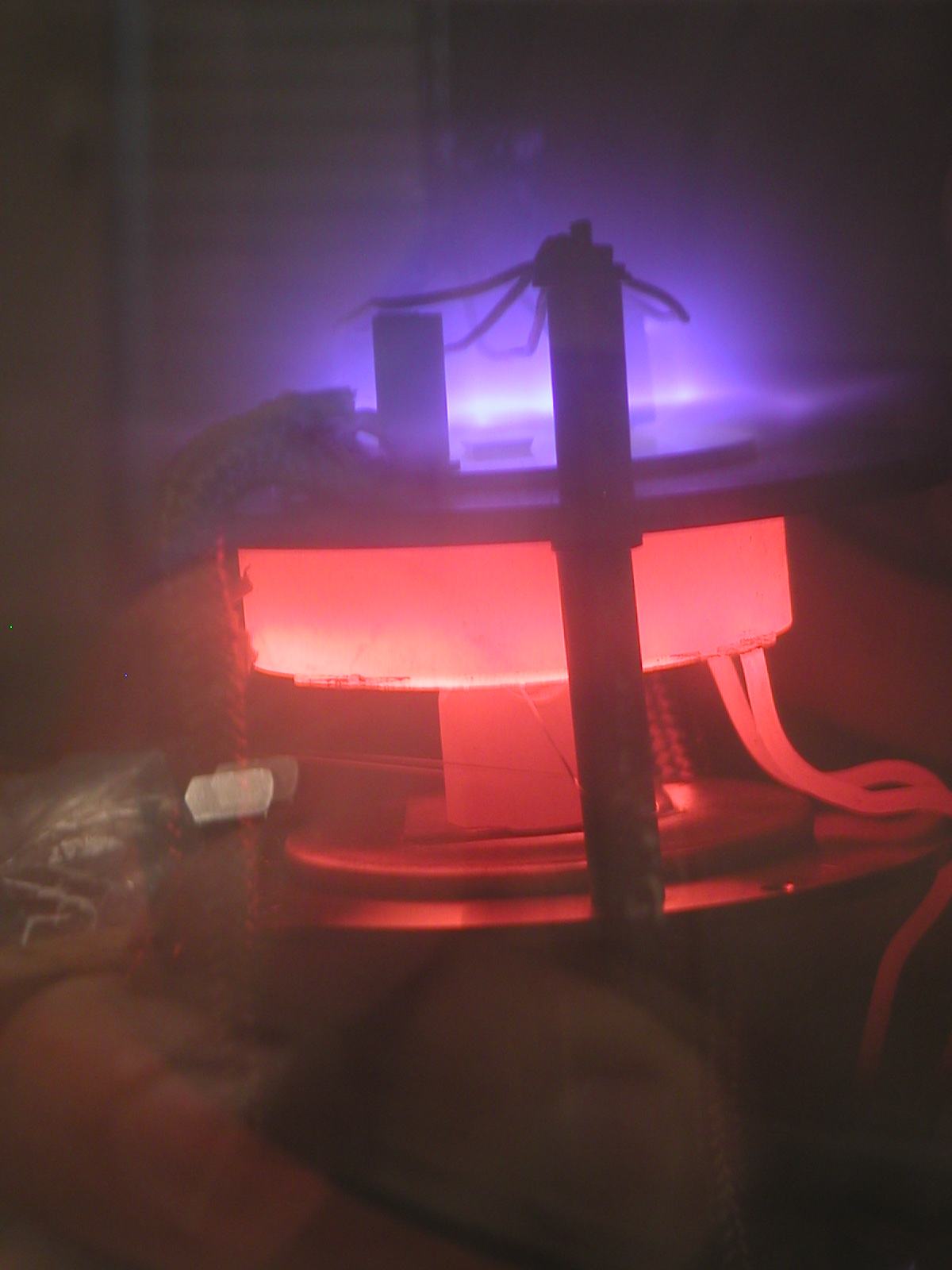
 DC plasma (violet) enhances the growth of carbon nanotubes in this laboratory-scale PECVD apparatus.
Chemical vapor deposition (CVD) is a chemical process used to produce high-purity, high-performance solid materials. The process is often used in the semiconductor industry to produce thin films. In a typical CVD process, the wafer (substrate) is exposed to one or more volatile precursors, which react and/or decompose on the substrate surface to produce the desired deposit. Frequently, volatile by-products are also produced, which are removed by gas flow through the reaction chamber.
Microfabrication processes widely use CVD to deposit materials in various forms, including: monocrystalline, polycrystalline, amorphous, and epitaxial. These materials include: silicon, carbon fiber, carbon nanofibers, filaments, carbon nanotubes, SiO2, silicon-germanium, tungsten, silicon carbide, silicon nitride, silicon oxynitride, titanium nitride, and various high-k dielectrics. The CVD process is also used to produce synthetic diamonds.
Contents
Types of chemical vapor deposition
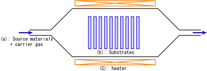
 Hot-wall thermal CVD (batch operation type)
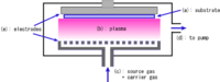 Plasma assisted CVD
A number of forms of CVD are in wide use and are frequently referenced in the literature. These processes differ in the means by which chemical reactions are initiated (e.g., activation process) and process conditions.
- Classified by operating pressure
- Atmospheric pressure CVD (APCVD) – CVD processes at atmospheric pressure.
- Low-pressure CVD (LPCVD) – CVD processes at subatmospheric pressures.[1] Reduced pressures tend to reduce unwanted gas-phase reactions and improve film uniformity across the wafer. Most modern CVD processes are either LPCVD or UHVCVD.
- Ultrahigh vacuum CVD (UHVCVD) – CVD processes at a very low pressure, typically below 10−6 Pa (~10−8 torr). Note that in other fields, a lower division between high and ultra-high vacuum is common, often 10−7 Pa.
- Classified by physical characteristics of vapor
- Aerosol assisted CVD (AACVD) – A CVD process in which the precursors are transported to the substrate by means of a liquid/gas aerosol, which can be generated ultrasonically. This technique is suitable for use with non-volatile precursors.
- Direct liquid injection CVD (DLICVD) – A CVD process in which the precursors are in liquid form (liquid or solid dissolved in a convenient solvent). Liquid solutions are injected in a vaporization chamber towards injectors (typically car injectors). Then the precursor vapors are transported to the substrate as in classical CVD process. This technique is suitable for use on liquid or solid precursors. High growth rates can be reached using this technique.
- Plasma methods (see also Plasma processing)
- Microwave plasma-assisted CVD (MPCVD)
- Plasma-Enhanced CVD (PECVD) – CVD processes that utilize plasma to enhance chemical reaction rates of the precursors.[2] PECVD processing allows deposition at lower temperatures, which is often critical in the manufacture of semiconductors.
- Remote plasma-enhanced CVD (RPECVD) – Similar to PECVD except that the wafer substrate is not directly in the plasma discharge region. Removing the wafer from the plasma region allows processing temperatures down to room temperature.
- Atomic layer CVD (ALCVD) – Deposits successive layers of different substances to produce layered, crystalline films. See Atomic layer epitaxy.
- Combustion Chemical Vapor Deposition (CCVD) – nGimat's proprietary Combustion Chemical Vapor Deposition process is an open-atmosphere, flame-based technique for depositing high-quality thin films and nanomaterials.
- Hot wire CVD (HWCVD) – also known as catalytic CVD (Cat-CVD) or hot filament CVD (HFCVD). Uses a hot filament to chemically decompose the source gases.[3]
- Metalorganic chemical vapor deposition (MOCVD) – CVD processes based on metalorganic precursors.
- Hybrid Physical-Chemical Vapor Deposition (HPCVD) – Vapor deposition processes that involve both chemical decomposition of precursor gas and vaporization of a solid source.
- Rapid thermal CVD (RTCVD) – CVD processes that use heating lamps or other methods to rapidly heat the wafer substrate. Heating only the substrate rather than the gas or chamber walls helps reduce unwanted gas phase reactions that can lead to particle formation.
- Vapor phase epitaxy (VPE)
Substances commonly deposited for ICs
This section discusses the CVD processes often used for integrated circuits (ICs). Particular materials are deposited best under particular conditions.
Polysilicon
Polycrystalline silicon is deposited from silane (SiH4), using the following reaction:
- SiH4 → Si + 2 H2
This reaction is usually performed in LPCVD systems, with either pure silane feedstock, or a solution of silane with 70–80% nitrogen. Temperatures between 600 and 650 °C and pressures between 25 and 150 Pa yield a growth rate between 10 and 20 nm per minute. An alternative process uses a hydrogen-based solution. The hydrogen reduces the growth rate, but the temperature is raised to 850 or even 1050 °C to compensate.
Polysilicon may be grown directly with doping, if gases such as phosphine, arsine or diborane are added to the CVD chamber. Diborane increases the growth rate, but arsine and phosphine decrease it.
Silicon dioxide
Silicon dioxide (usually called simply "oxide" in the semiconductor industry) may be deposited by several different processes. Common source gases include silane and oxygen, dichlorosilane (SiCl2H2) and nitrous oxide (N2O), or tetraethylorthosilicate (TEOS; Si(OC2H5)4). The reactions are as follows[citation needed]:
- SiH4 + O2 → SiO2 + 2 H2
- SiCl2H2 + 2 N2O → SiO2 + 2 N2 + 2 HCl
- Si(OC2H5)4 → SiO2 + byproducts
The choice of source gas depends on the thermal stability of the substrate; for instance, aluminium is sensitive to high temperature. Silane deposits between 300 and 500 °C, dichlorosilane at around 900 °C, and TEOS between 650 and 750 °C, resulting in a layer of low- temperature oxide (LTO). However, silane produces a lower-quality oxide than the other methods (lower dielectric strength, for instance), and it deposits nonconformally. Any of these reactions may be used in LPCVD, but the silane reaction is also done in APCVD. CVD oxide invariably has lower quality than thermal oxide, but thermal oxidation can only be used in the earliest stages of IC manufacturing.
Oxide may also be grown with impurities (alloying or "doping"). This may have two purposes. During further process steps that occur at high temperature, the impurities may diffuse from the oxide into adjacent layers (most notably silicon) and dope them. Oxides containing 5–15% impurities by mass are often used for this purpose. In addition, silicon dioxide alloyed with phosphorus pentoxide ("P-glass") can be used to smooth out uneven surfaces. P-glass softens and reflows at temperatures above 1000 °C. This process requires a phosphorus concentration of at least 6%, but concentrations above 8% can corrode aluminium. Phosphorus is deposited from phosphine gas and oxygen:
- 4 PH3 + 5 O2 → 2 P2O5 + 6 H2
Glasses containing both boron and phosphorus (borophosphosilicate glass, BPSG) undergo viscous flow at lower temperatures; around 850 °C is achievable with glasses containing around 5 weight % of both constituents, but stability in air can be difficult to achieve. Phosphorus oxide in high concentrations interacts with ambient moisture to produce phosphoric acid. Crystals of BPO4 can also precipitate from the flowing glass on cooling; these crystals are not readily etched in the standard reactive plasmas used to pattern oxides, and will result in circuit defects in integrated circuit manufacturing.
Besides these intentional impurities, CVD oxide may contain byproducts of the deposition process. TEOS produces a relatively pure oxide, whereas silane introduces hydrogen impurities, and dichlorosilane introduces chlorine.
Lower temperature deposition of silicon dioxide and doped glasses from TEOS using ozone rather than oxygen has also been explored (350 to 500 °C). Ozone glasses have excellent conformality but tend to be hygroscopic – that is, they absorb water from the air due to the incorporation of silanol (Si-OH) in the glass. Infrared spectroscopy and mechanical strain as a function of temperature are valuable diagnostic tools for diagnosing such problems.
Silicon nitride
Silicon nitride is often used as an insulator and chemical barrier in manufacturing ICs. The following two reactions deposit nitride from the gas phase:
- 3 SiH4 + 4 NH3 → Si3N4 + 12 H2
- 3 SiCl2H2 + 4 NH3 → Si3N4 + 6 HCl + 6 H2
Silicon nitride deposited by LPCVD contains up to 8% hydrogen. It also experiences strong tensile stress, which may crack films thicker than 200 nm. However, it has higher resistivity and dielectric strength than most insulators commonly available in microfabrication (1016 Ω·cm and 10 MV/cm, respectively).
Another two reactions may be used in plasma to deposit SiNH:
- 2 SiH4 + N2 → 2 SiNH + 3 H2
- SiH4 + NH3 → SiNH + 3 H2
These films have much less tensile stress, but worse electrical properties (resistivity 106 to 1015 Ω·cm, and dielectric strength 1 to 5 MV/cm).[4]
Metals
Some metals (notably aluminium and copper) are seldom or never deposited by CVD. As of 2010[update], a commercially, cost effective, viable CVD process for copper did not exist, though copper formate, copper(hfac)2, Cu(II) ethyl acetoacetate, and other precursors have been used. Copper deposition of the metal has been done mostly by electroplating, in order to reduce the cost. Aluminum can be deposited from tri-isobutyl aluminium (TIBAL), tri ethyl/methyl aluminum (TEA,TMA), or dimethylaluminum hydride (DMAH), but physical vapor deposition methods are usually preferred.[citation needed]
However, CVD processes for molybdenum, tantalum, titanium, nickel, and tungsten are widely used[citation needed]. These metals can form useful silicides when deposited onto silicon. Mo, Ta and Ti are deposited by LPCVD, from their pentachlorides. Nickel, molybdenum, and tungsten can be deposited at low temperatures from their carbonyl precursors. In general, for an arbitrary metal M, the reaction is as follows:
- 2 MCl5 + 5 H2 → 2 M + 10 HCl
The usual source for tungsten is tungsten hexafluoride, which may be deposited in two ways:
- WF6 → W + 3 F2
- WF6 + 3 H2 → W + 6 HF
See also
- Atomic layer deposition, a more precise and conformal coating technology
- Carbonyl metallurgy
- Electrostatic spray assisted vapor deposition
- Ion plating, a process that may use chemical vapor precursors
- Bubbler cylinder
References
- ^ Low Pressure Chemical Vapor Deposition – Technology and Equipment, http://www.crystec.com/klllpcvde.htm
- ^ Plasma Enhanced Chemical Vapor Deposition – Technology and Equipment, http://www.crystec.com/tridepe.htm
- ^ Schropp, R.E.I.; B. Stannowski, A.M. Brockhoff, P.A.T.T. van Veenendaal and J.K. Rath. "Hot wire CVD of heterogeneous and polycrystalline silicon semiconducting thin films for application in thin film transistors and solar cells" (PDF). Materials Physics and Mechanics. pp. 73–82. http://www.ipme.ru/e-journals/MPM/no_2100/schropp/schropp.pdf.
- ^ S.M. Sze (2008). Semiconductor devices: physics and technology. Wiley-India. p. 384. ISBN 812651681X.
Further reading
- Jaeger, Richard C. (2002). "Film Deposition". Introduction to Microelectronic Fabrication. Upper Saddle River: Prentice Hall. ISBN 0-201-44494-7.
- Smith, Donald (1995). Thin-Film Deposition: Principles and Practice. MacGraw-Hill. ISBN 0070585024.
- Dobkin and Zuraw (2003). Principles of Chemical Vapor Deposition. Kluwer. ISBN 1402012489.
External links
- Fundamentals of Chemical Vapor Deposition, by TimeDomain CVD, Inc.
- Traditional Coating Technologies
Categories:- Plasma processing
- Semiconductor device fabrication
- Chemical processes
- Coatings
- Thin film deposition
- Vacuum
- Glass coating and surface modification
- Classified by operating pressure

Wikimedia Foundation. 2010.