- Chemical vapor deposition of diamond
-
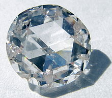 Colorless gem cut from diamond grown by chemical vapor deposition
Chemical vapor deposition of diamond or CVD is a method of producing synthetic diamond by creating the circumstances necessary for carbon atoms in a gas to settle on a substrate in crystalline form.
Chemical vapor deposition of diamond has received a great deal of attention in the materials sciences because it allows many new applications of diamond that had previously been considered too difficult to make economical. CVD diamond growth typically occurs under low pressure (1–27 kPa; 0.145–3.926 psi; 7.5-203 Torr) and involves feeding varying amounts of gases into a chamber, energizing them and providing conditions for diamond growth on the substrate. The gases always include a carbon source, and typically include hydrogen as well, though the amounts used vary greatly depending on the type of diamond being grown. Energy sources include hot filament, microwave power, and arc discharges, among others. The energy source is intended to generate a plasma in which the gases are broken down and more complex chemistries occur. The actual chemical process for diamond growth is still under study and is complicated by the very wide variety of diamond growth processes used.
The advantages to CVD diamond growth include the ability to grow diamond over large areas, the ability to grow diamond on a substrate, and the control over the properties of the diamond produced. In the past, when high pressure high temperature (HPHT) techniques were used to produce diamond, the diamonds were typically very small free standing diamonds of varying sizes. With CVD diamond growth areas of greater than fifteen centimeters (six inches) diameter have been achieved and much larger areas are likely to be successfully coated with diamond in the future. Improving this ability is key to enabling several important applications.
The ability to grow diamond directly on a substrate is important because it allows the addition of many of diamond’s important qualities to other materials. Since diamond has the highest thermal conductivity of any bulk material, layering diamond onto high heat producing electronics (such as optics and transistors) allows the diamond to be used as a heat sink[1][2]. Diamond films are being grown on valve rings, cutting tools, and other objects that benefit from diamond’s hardness and exceedingly low wear rate. In each case the diamond growth must be carefully done to achieve the necessary adhesion onto the substrate. Diamond's very high scratch resistance and thermal conductivity, combined with a lower coefficient of thermal expansion than Pyrex glass, a coefficient of friction close to that of Teflon (Polytetrafluoroethylene) and strong lipophilicity would make it a nearly ideal non-stick coating for cookware if large substrate areas could be coated economically.
The most important attribute of CVD diamond growth is the ability to control the properties of the diamond produced. In the area of diamond growth the word “diamond” is used as a description of any material primarily made up of sp3 bonded carbon, and there are many different types of diamond included in this. By regulating the processing parameters—especially the gases introduced, but also including the pressure the system is operated under, the temperature of the diamond, and the method of generating plasma—many different materials that can be considered diamond can be made. Single crystal diamond can be made containing various dopants[3]. Polycrystalline diamond consisting of grain sizes from several nanometers to several micrometers can be grown[4][5]. Some polycrystalline diamond grains are surrounded by thin, non-diamond carbon, while others are not. These different factors affect the diamond’s hardness, smoothness, conductivity, optical properties and more.
See also
References
- ^ Costello, M; Tossell, D; Reece, D; Brierley, C; Savage, J (1994). "Diamond protective coatings for optical components☆". Diamond and Related Materials 3 (8): 1137–1141. doi:10.1016/0925-9635(94)90108-2.
- ^ Sun Lee, Woong; Yu, Jin (2005). "Comparative study of thermally conductive fillers in underfill for the electronic components". Diamond and Related Materials 14 (10): 1647–1653. doi:10.1016/j.diamond.2005.05.008.
- ^ Isberg, J (2004). "Single crystal diamond for electronic applications". Diamond and Related Materials 13 (2): 320–324. doi:10.1016/j.diamond.2003.10.017.
- ^ Costello, M; Tossell, D; Reece, D; Brierley, C; Savage, J (1994). "Diamond protective coatings for optical components☆". Diamond and Related Materials 3 (8): 1137–1141. doi:10.1016/0925-9635(94)90108-2.
- ^ Krauss, A (2001). "Ultrananocrystalline diamond thin films for MEMS and moving mechanical assembly devices". Diamond and Related Materials 10 (11): 1952–1961. doi:10.1016/S0925-9635(01)00385-5.
Further reading
- K. Okada "Plasma-enhanced chemical vapor deposition of nanocrystalline diamond" Sci. Technol. Adv. Mater. 8 (2007) 624 free-download review
- T. Liu, D. Raabe and S. Zaefferer "A 3D tomographic EBSD analysis of a CVD diamond thin film" Sci. Technol. Adv. Mater. 9 (2008) 035013 free-download
- Christoph Wild "CVD Diamond Properties and useful Formula" CVD Diamond Booklet (2008) PDF free-download
Categories:- Industrial processes
- Synthetic diamond

Wikimedia Foundation. 2010.