- CPU cache
-
A CPU cache is a cache used by the central processing unit of a computer to reduce the average time to access memory. The cache is a smaller, faster memory which stores copies of the data from the most frequently used main memory locations. As long as most memory accesses are cached memory locations, the average latency of memory accesses will be closer to the cache latency than to the latency of main memory.
When the processor needs to read from or write to a location in main memory, it first checks whether a copy of that data is in the cache. If so, the processor immediately reads from or writes to the cache, which is much faster than reading from or writing to main memory.
Most modern desktop and server CPUs have at least three independent caches: an instruction cache to speed up executable instruction fetch, a data cache to speed up data fetch and store, and a translation lookaside buffer (TLB) used to speed up virtual-to-physical address translation for both executable instructions and data. Data cache is usually organized as a hierarchy of more cache levels (L1, L2, etc.; see Multi-level caches).
Contents
Details of operation
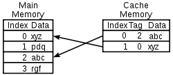
This section describes typical data cache and some instruction caches; A TLB may have more complexity and an instruction cache may be simpler. The diagram on the right shows two memories. Each location in each memory contains data (a cache line or cache block), the size of which is usually larger than the size of the largest common access requested by a CPU instruction[1]. Such accesses are typically the size of a register (e.g., 2 bytes for a PDP-11, 4 bytes for a general purpose register and 8 bytes for a floating-point register in the MIPS architecture, 16 bytes for a XMM register in x86 processors with SSE). (The PDP-11/73 had a 2 byte cache line[2] while the POWER4 L3 cache had lines of 512 bytes[3].) Each location in each memory also has an index, which is a unique number used to refer to that location. The index for a location in main memory is called a physical address. Each location in the cache has a tag that contains the index of the datum in main memory that has been cached.
When the processor needs to read or write a location in main memory, it first checks whether that memory location is in the cache. This is accomplished by comparing the address of the memory location to all tags in the cache that might contain that address. If the processor finds that the memory location is in the cache, we say that a cache hit has occurred; otherwise, we speak of a cache miss. In the case of a cache hit, the processor immediately reads or writes the data in the cache line. The proportion of accesses that result in a cache hit is known as the hit rate, and is a measure of the effectiveness of the cache for a given program or algorithm.
In the case of a miss, the cache allocates a new entry, which comprises the tag just missed and a copy of the data. The reference can then be applied to the new entry just as in the case of a hit. Read misses delay execution because they require data to be transferred from a much slower memory than the cache itself. Write misses may occur without such penalty since the data can be copied in the background. Instruction caches are similar to data caches but the CPU only performs read accesses (instruction fetch) to the instruction cache. Instruction and data caches can be separated for higher performance with Harvard CPUs but they can also be combined to reduce the hardware overhead.
In order to make room for the new entry on a cache miss, the cache has to evict one of the existing entries. The heuristic that it uses to choose the entry to evict is called the replacement policy. The fundamental problem with any replacement policy is that it must predict which existing cache entry is least likely to be used in the future. Predicting the future is difficult, especially for hardware caches that use simple rules amenable to implementation in circuitry, so there are a variety of replacement policies to choose from and no perfect way to decide among them. One popular replacement policy, LRU, replaces the least recently used entry. Defining some memory ranges non cacheable avoids affecting performance by storing in caches information which are never re-used or seldom used. Cache misses are simply ignored for not cacheable data. Cache entries may also be disabled or locked depending on the context.
If data are written to the cache, they must at some point be written to main memory as well. The timing of this write is controlled by what is known as the write policy. In a write-through cache, every write to the cache causes a write to main memory. Alternatively, in a write-back or copy-back cache, writes are not immediately mirrored to the main memory. Instead, the cache tracks which locations have been written over (these locations are marked dirty). The data in these locations are written back to the main memory when that data is evicted from the cache. For this reason, a miss in a write-back cache may sometimes require two memory accesses to service: one to first write the dirty location to memory and then another to read the new location from memory.
There are intermediate policies as well. The cache may be write-through, but the writes may be held in a store data queue temporarily, usually so that multiple stores can be processed together (which can reduce bus turnarounds and so improve bus utilization).
The data in main memory being cached may be changed by other entities (e.g. peripherals using direct memory access or multi-core processor), in which case the copy in the cache may become out-of-date or stale. Alternatively, when the CPU in a multi-core processor updates the data in the cache, copies of data in caches associated with other cores will become stale. Communication protocols between the cache managers which keep the data consistent are known as cache coherence protocols. Another possibility is to share non cacheable data.
The time taken to fetch one datum from memory (read latency) matters because the CPU will run out of things to do while waiting for the datum. When a CPU reaches this state, it is called a stall. As CPUs become faster, stalls due to cache misses displace more potential computation; modern CPUs can execute hundreds of instructions in the time taken to fetch a single datum from the main memory. Various techniques have been employed to keep the CPU busy during this time. Out-of-order CPUs (Pentium Pro and later Intel designs, for example) attempt to execute independent instructions after the instruction that is waiting for the cache miss data. Another technology, used by many processors, is simultaneous multithreading (SMT), or -in Intel's terminology- hyper-threading (HT), which allows an alternate thread to use the CPU core while a first thread waits for data to come from main memory.
Cache entry structure
Cache row entries usually have the following structure:
tag data blocks valid bit The data blocks (cache line) contain the actual data fetched from the main memory. The valid bit (dirty bit) denotes that this particular entry has valid data.
An effective memory address is split (MSB to LSB) into the tag, the index and the displacement (offset),
tag index displacement The index describes which row the data has been put in. The index length is
 bits. The displacement (offset) specifies which block of the stored data blocks from the cache row is needed. The displacement length is
  bits. The tag contains the most significant bits of the address, which are checked against the current row (the row has been retrieved by index) to see if it is the one we need or another, irrelevant memory location that happened to have the same index bits as the one we want. The tag length in bits is address_length − index_length − displacement_length.
Associativity
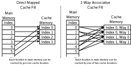 Which memory locations can be cached by which cache locations
The replacement policy decides where in the cache a copy of a particular entry of main memory will go. If the replacement policy is free to choose any entry in the cache to hold the copy, the cache is called fully associative. At the other extreme, if each entry in main memory can go in just one place in the cache, the cache is direct mapped. Many caches implement a compromise in which each entry in main memory can go to any one of N places in the cache, and are described as N-way set associative. For example, the level-1 data cache in an AMD Athlon is 2-way set associative, which means that any particular location in main memory can be cached in either of 2 locations in the level-1 data cache.
Associativity is a trade-off. If there are ten places to which the replacement policy could have mapped a memory location, then to check if that location is in the cache, ten cache entries must be searched. Checking more places takes more power, chip area, and potentially time. On the other hand, caches with more associativity suffer fewer misses (see conflict misses, below), so that the CPU wastes less time reading from the slow main memory. The rule of thumb is that doubling the associativity, from direct mapped to 2-way, or from 2-way to 4-way, has about the same effect on hit rate as doubling the cache size. Associativity increases beyond 4-way have much less effect on the hit rate,[4] and are generally done for other reasons (see virtual aliasing, below).
In order of worse but simple to better but complex:
- direct mapped cache—the best (fastest) hit times, and so the best tradeoff for "large" caches
- 2-way set associative cache
- 2-way skewed associative cache – "the best tradeoff for .... caches whose sizes are in the range 4K-8K bytes" – André Seznec[5]
- 4-way set associative cache
- fully associative cache – the best (lowest) miss rates, and so the best tradeoff when the miss penalty is very high
Direct-mapped cache
Here each datum can only go in one entry. It doesn't have a replacement policy as such, since there is no choice of which datum to evict. This means that if two locations map to the same entry, they may continually knock each other out. Although simpler, a direct-mapped cache needs to be much larger than an associative one to give comparable performance, and is more unpredictable.
2-way set associative cache
If each location in main memory can be cached in either of two locations in the cache, one logical question is: which two? The simplest and most commonly used scheme, shown in the right-hand diagram above, is to use the least significant bits of the memory location's index as the index for the cache memory, and to have two entries for each index. One benefit of this scheme is that the tags stored in the cache do not have to include that part of the main memory address which is implied by the cache memory's index. Since the cache tags are fewer bits, they take less area on the microprocessor chip and can be read and compared faster. Also LRU is especially simple since only one bit needs to be stored for each pair.
Speculative execution
One of the advantages of a direct mapped cache is that it allows simple and fast speculation. Once the address has been computed, the one cache index which might have a copy of that datum is known. That cache entry can be read, and the processor can continue to work with that data before it finishes checking that the tag actually matches the requested address.
The idea of having the processor use the cached data before the tag match completes can be applied to associative caches as well. A subset of the tag, called a hint, can be used to pick just one of the possible cache entries mapping to the requested address. This datum can then be used in parallel with checking the full tag. The hint technique works best when used in the context of address translation, as explained below.
2-way skewed associative cache
Other schemes have been suggested, such as the skewed cache,[5] where the index for way 0 is direct, as above, but the index for way 1 is formed with a hash function. A good hash function has the property that addresses which conflict with the direct mapping tend not to conflict when mapped with the hash function, and so it is less likely that a program will suffer from an unexpectedly large number of conflict misses due to a pathological access pattern. The downside is extra latency from computing the hash function.[6] Additionally, when it comes time to load a new line and evict an old line, it may be difficult to determine which existing line was least recently used, because the new line conflicts with data at different indexes in each way; LRU tracking for non-skewed caches is usually done on a per-set basis. Nevertheless, skewed-associative caches have major advantages over conventional set-associative ones.[7]
Pseudo-associative cache
A true set-associative cache tests all the possible ways simultaneously, using something like a content addressable memory. A pseudo-associative cache tests each possible way one at a time. A hash-rehash cache is one kind of pseudo-associative cache.
In the common case of finding a hit in the first way tested, a pseudo-associative cache is as fast as a direct-mapped cache. But it has a much lower conflict miss rate than a direct-mapped cache, closer to the miss rate of a fully associative cache. [6]
Cache miss
A cache miss refers to a failed attempt to read or write a piece of data in the cache, which results in a main memory access with much longer latency. There are three kinds of cache misses: instruction read miss, data read miss, and data write miss.
A cache read miss from an instruction cache generally causes the most delay, because the processor, or at least the thread of execution, has to wait (stall) until the instruction is fetched from main memory.
A cache read miss from a data cache usually causes less delay, because instructions not dependent on the cache read can be issued and continue execution until the data is returned from main memory, and the dependent instructions can resume execution.
A cache write miss to a data cache generally causes the least delay, because the write can be queued and there are few limitations on the execution of subsequent instructions. The processor can continue until the queue is full.
In order to lower cache miss rate, a great deal of analysis has been done on cache behavior in an attempt to find the best combination of size, associativity, block size, and so on. Sequences of memory references performed by benchmark programs are saved as address traces. Subsequent analyses simulate many different possible cache designs on these long address traces. Making sense of how the many variables affect the cache hit rate can be quite confusing. One significant contribution to this analysis was made by Mark Hill, who separated misses into three categories (known as the Three Cs):
- Compulsory misses are those misses caused by the first reference to a datum. Cache size and associativity make no difference to the number of compulsory misses. Prefetching can help here, as can larger cache block sizes (which are a form of prefetching). Compulsory misses are sometimes referred to as cold misses.
- Capacity misses are those misses that occur regardless of associativity or block size, solely due to the finite size of the cache. The curve of capacity miss rate versus cache size gives some measure of the temporal locality of a particular reference stream. Note that there is no useful notion of a cache being "full" or "empty" or "near capacity": CPU caches almost always have nearly every line filled with a copy of some line in main memory, and nearly every allocation of a new line requires the eviction of an old line.
- Conflict misses are those misses that could have been avoided, had the cache not evicted an entry earlier. Conflict misses can be further broken down into mapping misses, that are unavoidable given a particular amount of associativity, and replacement misses, which are due to the particular victim choice of the replacement policy.
 Miss rate versus cache size on the Integer portion of SPEC CPU2000
The graph to the right summarizes the cache performance seen on the Integer portion of the SPEC CPU2000 benchmarks, as collected by Hill and Cantin.[8] These benchmarks are intended to represent the kind of workload that an engineering workstation computer might see on any given day. The reader should keep in mind that finding benchmarks which are even usefully representative of many programs has been very difficult, and there will always be important programs with very different behavior than what is shown here.
We can see the different effects of the three Cs in this graph.
At the far right, with cache size labelled "Inf", we have the compulsory misses. If we wish to improve a machine's performance on SpecInt2000, increasing the cache size beyond 1 MB is essentially futile. That's the insight given by the compulsory misses.
The fully associative cache miss rate here is almost representative of the capacity miss rate. The difference is that the data presented is from simulations assuming an LRU replacement policy. Showing the capacity miss rate would require a perfect replacement policy, i.e. an oracle that looks into the future to find a cache entry which is actually not going to be hit.
Note that our approximation of the capacity miss rate falls steeply between 32 kB and 64 kB. This indicates that the benchmark has a working set of roughly 64 kB. A CPU cache designer examining this benchmark will have a strong incentive to set the cache size to 64 kB rather than 32 kB. Note that, on this benchmark, no amount of associativity can make a 32 kB cache perform as well as a 64 kB 4-way, or even a direct-mapped 128 kB cache.
Finally, note that between 64 kB and 1 MB there is a large difference between direct-mapped and fully associative caches. This difference is the conflict miss rate. The insight from looking at conflict miss rates is that secondary caches benefit a great deal from high associativity.
This benefit was well known in the late 80s and early 90s, when CPU designers could not fit large caches on-chip, and could not get sufficient bandwidth to either the cache data memory or cache tag memory to implement high associativity in off-chip caches. Desperate hacks were attempted: the MIPS R8000 used expensive off-chip dedicated tag SRAMs, which had embedded tag comparators and large drivers on the match lines, in order to implement a 4 MB 4-way associative cache. The MIPS R10000 used ordinary SRAM chips for the tags. Tag access for both ways took two cycles. To reduce latency, the R10000 would guess which way of the cache would hit on each access.
Address translation
Most general purpose CPUs implement some form of virtual memory. To summarize, each program running on the machine sees its own simplified address space, which contains code and data for that program only. Each program uses this virtual address space without regard for where it exists in physical memory.
Virtual memory requires the processor to translate virtual addresses generated by the program into physical addresses in main memory. The portion of the processor that does this translation is known as the memory management unit (MMU). The fast path through the MMU can perform those translations stored in the translation lookaside buffer (TLB), which is a cache of mappings from the operating system's page table.
For the purposes of the present discussion, there are three important features of address translation:
- Latency: The physical address is available from the MMU some time, perhaps a few cycles, after the virtual address is available from the address generator.
- Aliasing: Multiple virtual addresses can map to a single physical address. Most processors guarantee that all updates to that single physical address will happen in program order. To deliver on that guarantee, the processor must ensure that only one copy of a physical address resides in the cache at any given time.
- Granularity: The virtual address space is broken up into pages. For instance, a 4 GB virtual address space might be cut up into 1048576 pages of 4 kB size, each of which can be independently mapped. There may be multiple page sizes supported; see virtual memory for elaboration.
A historical note: some early virtual memory systems were very slow, because they required an access to the page table (held in main memory) before every programmed access to main memory.[NB 1] With no caches, this effectively cut the speed of the machine in half. The first hardware cache used in a computer system was not actually a data or instruction cache, but rather a TLB.
Caches can be divided into 4 types, based on whether the index or tag correspond to physical or virtual addresses:
- Physically indexed, physically tagged (PIPT) caches use the physical address for both the index and the tag. While this is simple and avoids problems with aliasing, it is also slow, as the physical address must be looked up (which could involve a TLB miss and access to main memory) before that address can be looked up in the cache.
- Virtually indexed, virtually tagged (VIVT) caches use the virtual address for both the index and the tag. This caching scheme can result in much faster lookups, since the MMU doesn't need to be consulted first to determine the physical address for a given virtual address. However, VIVT suffers from aliasing problems, where several different virtual addresses may refer to the same physical address. The result is that such addresses would be cached separately despite referring to the same memory, causing coherency problems. Another problem is homonyms, where the same virtual address maps to several different physical addresses. It is not possible to distinguish these mappings by only looking at the virtual index, though potential solutions include: flushing the cache after a context switch, forcing address spaces to be non-overlapping, tagging the virtual address with an address space ID (ASID), or using physical tags. Additionally, there is a problem that virtual-to-physical mappings can change, which would require flushing cache lines, as the VAs would no longer be valid.
- Virtually indexed, physically tagged (VIPT) caches use the virtual address for the index and the physical address in the tag. The advantage over PIPT is lower latency, as the cache line can be looked up in parallel with the TLB translation, however the tag can't be compared until the physical address is available. The advantage over VIVT is that since the tag has the physical address, the cache can detect homonyms. VIPT requires more tag bits, as the index bits no longer represent the same address.
- Physically indexed, virtually tagged caches are only theoretical as they would basically be useless.[11]
The speed of this recurrence (the load latency) is crucial to CPU performance, and so most modern level-1 caches are virtually indexed, which at least allows the MMU's TLB lookup to proceed in parallel with fetching the data from the cache RAM.
But virtual indexing is not the best choice for all cache levels. The cost of dealing with virtual aliases grows with cache size, and as a result most level-2 and larger caches are physically indexed.
Caches have historically used both virtual and physical addresses for the cache tags, although virtual tagging is now uncommon. If the TLB lookup can finish before the cache RAM lookup, then the physical address is available in time for tag compare, and there is no need for virtual tagging. Large caches, then, tend to be physically tagged, and only small, very low latency caches are virtually tagged. In recent general-purpose CPUs, virtual tagging has been superseded by vhints, as described below.
Homonym and synonym problems
The cache that relies on the virtual indexing and tagging becomes inconsistent after the same virtual address is mapped into different physical addresses (homonym). This can be solved by using physical address for tagging or by storing the address space id in the cache line. However the latter of these two approaches does not help against the synonym problem, where several cache lines end up storing data for the same physical address. Writing to such location may update only one location in the cache, leaving others with inconsistent data. This problem might be solved by using non overlapping memory layouts for different address spaces or otherwise the cache (or part of it) must be flushed when the mapping changes.[12]
Virtual tags and vhints
The great advantage of virtual tags is that, for associative caches, they allow the tag match to proceed before the virtual to physical translation is done. However,
- coherence probes and evictions present a physical address for action. The hardware must have some means of converting the physical addresses into a cache index, generally by storing physical tags as well as virtual tags. For comparison, a physically tagged cache does not need to keep virtual tags, which is simpler.
- When a virtual to physical mapping is deleted from the TLB, cache entries with those virtual addresses will have to be flushed somehow. Alternatively, if cache entries are allowed on pages not mapped by the TLB, then those entries will have to be flushed when the access rights on those pages are changed in the page table.
It is also possible for the operating system to ensure that no virtual aliases are simultaneously resident in the cache. The operating system makes this guarantee by enforcing page coloring, which is described below. Some early RISC processors (SPARC, RS/6000) took this approach. It has not been used recently, as the hardware cost of detecting and evicting virtual aliases has fallen and the software complexity and performance penalty of perfect page coloring has risen.
It can be useful to distinguish the two functions of tags in an associative cache: they are used to determine which way of the entry set to select, and they are used to determine if the cache hit or missed. The second function must always be correct, but it is permissible for the first function to guess, and get the wrong answer occasionally.
Some processors (e.g. early SPARCs) have caches with both virtual and physical tags. The virtual tags are used for way selection, and the physical tags are used for determining hit or miss. This kind of cache enjoys the latency advantage of a virtually tagged cache, and the simple software interface of a physically tagged cache. It bears the added cost of duplicated tags, however. Also, during miss processing, the alternate ways of the cache line indexed have to be probed for virtual aliases and any matches evicted.
The extra area (and some latency) can be mitigated by keeping virtual hints with each cache entry instead of virtual tags. These hints are a subset or hash of the virtual tag, and are used for selecting the way of the cache from which to get data and a physical tag. Like a virtually tagged cache, there may be a virtual hint match but physical tag mismatch, in which case the cache entry with the matching hint must be evicted so that cache accesses after the cache fill at this address will have just one hint match. Since virtual hints have fewer bits than virtual tags distinguishing them from one another, a virtually hinted cache suffers more conflict misses than a virtually tagged cache.
Perhaps the ultimate reduction of virtual hints can be found in the Pentium 4 (Willamette and Northwood cores). In these processors the virtual hint is effectively 2 bits, and the cache is 4-way set associative. Effectively, the hardware maintains a simple permutation from virtual address to cache index, so that no content-addressable memory (CAM) is necessary to select the right one of the four ways fetched.
Page coloring
Large physically indexed caches (usually secondary caches) run into a problem: the operating system rather than the application controls which pages collide with one another in the cache. Differences in page allocation from one program run to the next lead to differences in the cache collision patterns, which can lead to very large differences in program performance. These differences can make it very difficult to get a consistent and repeatable timing for a benchmark run.
To understand the problem, consider a CPU with a 1 MB physically indexed direct-mapped level-2 cache and 4 kB virtual memory pages. Sequential physical pages map to sequential locations in the cache until after 256 pages the pattern wraps around. We can label each physical page with a color of 0–255 to denote where in the cache it can go. Locations within physical pages with different colors cannot conflict in the cache.
A programmer attempting to make maximum use of the cache may arrange his program's access patterns so that only 1 MB of data need be cached at any given time, thus avoiding capacity misses. But he should also ensure that the access patterns do not have conflict misses. One way to think about this problem is to divide up the virtual pages the program uses and assign them virtual colors in the same way as physical colors were assigned to physical pages before. The programmer can then arrange the access patterns of his code so that no two pages with the same virtual color are in use at the same time. There is a wide literature on such optimizations (e.g. loop nest optimization), largely coming from the High Performance Computing (HPC) community.
The snag is that while all the pages in use at any given moment may have different virtual colors, some may have the same physical colors. In fact, if the operating system assigns physical pages to virtual pages randomly and uniformly, it is extremely likely that some pages will have the same physical color, and then locations from those pages will collide in the cache (this is the birthday paradox).
The solution is to have the operating system attempt to assign different physical color pages to different virtual colors, a technique called page coloring. Although the actual mapping from virtual to physical color is irrelevant to system performance, odd mappings are difficult to keep track of and have little benefit, so most approaches to page coloring simply try to keep physical and virtual page colors the same.
If the operating system can guarantee that each physical page maps to only one virtual color, then there are no virtual aliases, and the processor can use virtually indexed caches with no need for extra virtual alias probes during miss handling. Alternatively, the O/S can flush a page from the cache whenever it changes from one virtual color to another. As mentioned above, this approach was used for some early SPARC and RS/6000 designs.
Cache hierarchy in a modern processor
Modern processors have multiple interacting caches on chip.
Specialized caches
Pipelined CPUs access memory from multiple points in the pipeline: instruction fetch, virtual-to-physical address translation, and data fetch (see classic RISC pipeline). The natural design is to use different physical caches for each of these points, so that no one physical resource has to be scheduled to service two points in the pipeline. Thus the pipeline naturally ends up with at least three separate caches (instruction, TLB, and data), each specialized to its particular role.
Pipelines with separate instruction and data caches, now predominant, are said to have a Harvard architecture. Originally, this phrase referred to machines with separate instruction and data memories, which proved not at all popular. Most modern CPUs have a single-memory von Neumann architecture.
Victim cache
A victim cache is a cache used to hold blocks evicted from a CPU cache upon replacement. The victim cache lies between the main cache and its refill path, and only holds blocks that were evicted from the main cache. The victim cache is usually fully associative, and is intended to reduce the number of conflict misses. Many commonly used programs do not require an associative mapping for all the accesses. In fact, only a small fraction of the memory accesses of the program require high associativity. The victim cache exploits this property by providing high associativity to only these accesses. It was introduced by Norman Jouppi in 1990.
Trace cache
One of the more extreme examples of cache specialization is the trace cache found in the Intel Pentium 4 microprocessors. A trace cache is a mechanism for increasing the instruction fetch bandwidth and decreasing power consumption (in the case of the Pentium 4) by storing traces of instructions that have already been fetched and decoded.
The earliest widely acknowledged academic publication of trace cache was by Eric Rotenberg, Steve Bennett, and Jim Smith in their 1996 paper "Trace Cache: a Low Latency Approach to High Bandwidth Instruction Fetching."[13]
An earlier publication is US Patent 5,381,533, "Dynamic flow instruction cache memory organized around trace segments independent of virtual address line", by Alex Peleg and Uri Weiser of Intel Corp., patent filed March 30, 1994, a continuation of an application filed in 1992, later abandoned.
A trace cache stores instructions either after they have been decoded, or as they are retired. Generally, instructions are added to trace caches in groups representing either individual basic blocks or dynamic instruction traces. A dynamic trace ("trace path") contains only instructions whose results are actually used, and eliminates instructions following taken branches (since they are not executed); a dynamic trace can be a concatenation of multiple basic blocks. This allows the instruction fetch unit of a processor to fetch several basic blocks, without having to worry about branches in the execution flow.
Trace lines are stored in the trace cache based on the program counter of the first instruction in the trace and a set of branch predictions. This allows for storing different trace paths that start on the same address, each representing different branch outcomes. In the instruction fetch stage of a pipeline, the current program counter along with a set of branch predictions is checked in the trace cache for a hit. If there is a hit, a trace line is supplied to fetch which does not have to go to a regular cache or to memory for these instructions. The trace cache continues to feed the fetch unit until the trace line ends or until there is a misprediction in the pipeline. If there is a miss, a new trace starts to be built.
Trace caches are also used in processors like the Intel Pentium 4 to store already decoded micro-operations, or translations of complex x86 instructions, so that the next time an instruction is needed, it does not have to be decoded again.
Multi-level caches
Another issue is the fundamental tradeoff between cache latency and hit rate. Larger caches have better hit rates but longer latency. To address this tradeoff, many computers use multiple levels of cache, with small fast caches backed up by larger slower caches.
Multi-level caches generally operate by checking the smallest Level 1 (L1) cache first; if it hits, the processor proceeds at high speed. If the smaller cache misses, the next larger cache (L2) is checked, and so on, before external memory is checked.
As the latency difference between main memory and the fastest cache has become larger, some processors have begun to utilize as many as three levels of on-chip cache. For example, the Alpha 21164 (1995) had 1 to 64MB off-chip L3 cache; the IBM POWER4 (2001) had a 256[citation needed]MB L3 cache off-chip, shared among several processors; the Itanium 2 (2003) had a 6 MB unified level 3 (L3) cache on-die; the Itanium 2 (2003) MX 2 Module incorporates two Itanium2 processors along with a shared 64 MB L4 cache on a MCM that was pin compatible with a Madison processor; Intel's Xeon MP product code-named "Tulsa" (2006) features 16 MB of on-die L3 cache shared between two processor cores; the AMD Phenom II (2008) has up to 6 MB on-die unified L3 cache; and the Intel Core i7 (2008) has an 8 MB on-die unified L3 cache that is inclusive, shared by all cores. The benefits of an L3 cache depend on the application's access patterns.
Finally, at the other end of the memory hierarchy, the CPU register file itself can be considered the smallest, fastest cache in the system, with the special characteristic that it is scheduled in software—typically by a compiler, as it allocates registers to hold values retrieved from main memory. (See especially loop nest optimization.) Register files sometimes also have hierarchy: The Cray-1 (circa 1976) had 8 address "A" and 8 scalar data "S" registers that were generally usable. There was also a set of 64 address "B" and 64 scalar data "T" registers that took longer to access, but were faster than main memory. The "B" and "T" registers were provided because the Cray-1 did not have a data cache. (The Cray-1 did, however, have an instruction cache.)
Multi-core chips
When considering a chip with multiple cores, there is a question of whether the caches should be shared or local to each core. Implementing shared cache undoubtedly introduces more wiring and complexity. But then, having one cache per chip, rather than core, greatly reduces the amount of space needed, and thus one can include a larger cache. Typically one finds that sharing L1 cache is undesirable since the latency increase is such that each core will run considerably slower than a single-core chip. But then, for the highest level (the last one called before accessing memory), having a global cache is desirable for several reasons. For example, an eight-core chip with three levels may include an L1 cache for each core, an L3 cache shared by all cores, with the L2 cache intermediate, e.g., one for each pair of cores.
Exclusive versus inclusive
Multi-level caches introduce new design decisions. For instance, in some processors, all data in the L1 cache must also be somewhere in the L2 cache. These caches are called strictly inclusive. Other processors (like the AMD Athlon) have exclusive caches — data is guaranteed to be in at most one of the L1 and L2 caches, never in both. Still other processors (like the Intel Pentium II, III, and 4), do not require that data in the L1 cache also reside in the L2 cache, although it may often do so. There is no universally accepted name for this intermediate policy.
The advantage of exclusive caches is that they store more data. This advantage is larger when the exclusive L1 cache is comparable to the L2 cache, and diminishes if the L2 cache is many times larger than the L1 cache. When the L1 misses and the L2 hits on an access, the hitting cache line in the L2 is exchanged with a line in the L1. This exchange is quite a bit more work than just copying a line from L2 to L1, which is what an inclusive cache does.
One advantage of strictly inclusive caches is that when external devices or other processors in a multiprocessor system wish to remove a cache line from the processor, they need only have the processor check the L2 cache. In cache hierarchies which do not enforce inclusion, the L1 cache must be checked as well. As a drawback, there is a correlation between the associativities of L1 and L2 caches: if the L2 cache does not have at least as many ways as all L1 caches together, the effective associativity of the L1 caches is restricted. Another disadvantage of inclusive cache is that whenever there is an eviction in L2 cache, the (possibly) corresponding lines in L1 also have to get evicted in order to maintain inclusiveness. This is quite a bit work, and would result in higher L1 miss rate.
Another advantage of inclusive caches is that the larger cache can use larger cache lines, which reduces the size of the secondary cache tags. (Exclusive caches require both caches to have the same size cache lines, so that cache lines can be swapped on a L1 miss, L2 hit). If the secondary cache is an order of magnitude larger than the primary, and the cache data is an order of magnitude larger than the cache tags, this tag area saved can be comparable to the incremental area needed to store the L1 cache data in the L2.
Example: the K8
To illustrate both specialization and multi-level caching, here is the cache hierarchy of the K8 core in the AMD Athlon 64 CPU.[14]
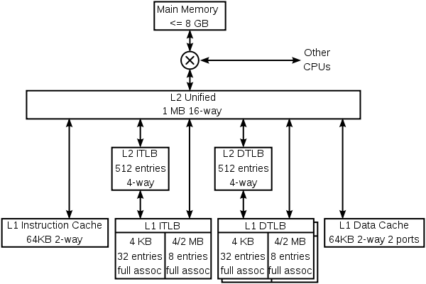 Example of hierarchy, the K8
The K8 has 4 specialized caches: an instruction cache, an instruction TLB, a data TLB, and a data cache. Each of these caches is specialized:
- The instruction cache keeps copies of 64-byte lines of memory, and fetches 16 bytes each cycle. Each byte in this cache is stored in ten bits rather than 8, with the extra bits marking the boundaries of instructions (this is an example of predecoding). The cache has only parity protection rather than ECC, because parity is smaller and any damaged data can be replaced by fresh data fetched from memory (which always has an up-to-date copy of instructions).
- The instruction TLB keeps copies of page table entries (PTEs). Each cycle's instruction fetch has its virtual address translated through this TLB into a physical address. Each entry is either 4 or 8 bytes in memory. Because the K8 has a variable page size, each of the TLBs is split into two sections, one to keep PTEs that map 4 kB pages, and one to keep PTEs that map 4 MB or 2 MB pages. The split allows the fully associative match circuitry in each section to be simpler. The operating system maps different sections of the virtual address space with different size PTEs.
- The data TLB has two copies which keep identical entries. The two copies allow two data accesses per cycle to translate virtual addresses to physical addresses. Like the instruction TLB, this TLB is split into two kinds of entries.
- The data cache keeps copies of 64-byte lines of memory. It is split into 8 banks (each storing 8 kB of data), and can fetch two 8-byte data each cycle so long as those data are in different banks. There are two copies of the tags, because each 64-byte line is spread among all 8 banks. Each tag copy handles one of the two accesses per cycle.
The K8 also has multiple-level caches. There are second-level instruction and data TLBs, which store only PTEs mapping 4 kB. Both instruction and data caches, and the various TLBs, can fill from the large unified L2 cache. This cache is exclusive to both the L1 instruction and data caches, which means that any 8-byte line can only be in one of the L1 instruction cache, the L1 data cache, or the L2 cache. It is, however, possible for a line in the data cache to have a PTE which is also in one of the TLBs—the operating system is responsible for keeping the TLBs coherent by flushing portions of them when the page tables in memory are updated.
The K8 also caches information that is never stored in memory—prediction information. These caches are not shown in the above diagram. As is usual for this class of CPU, the K8 has fairly complex branch prediction, with tables that help predict whether branches are taken and other tables which predict the targets of branches and jumps. Some of this information is associated with instructions, in both the level 1 instruction cache and the unified secondary cache.
The K8 uses an interesting trick to store prediction information with instructions in the secondary cache. Lines in the secondary cache are protected from accidental data corruption (e.g. by an alpha particle strike) by either ECC or parity, depending on whether those lines were evicted from the data or instruction primary caches. Since the parity code takes fewer bits than the ECC code, lines from the instruction cache have a few spare bits. These bits are used to cache branch prediction information associated with those instructions. The net result is that the branch predictor has a larger effective history table, and so has better accuracy.
More hierarchies
Other processors have other kinds of predictors (e.g. the store-to-load bypass predictor in the DEC Alpha 21264), and various specialized predictors are likely to flourish in future processors.
These predictors are caches in that they store information that is costly to compute. Some of the terminology used when discussing predictors is the same as that for caches (one speaks of a hit in a branch predictor), but predictors are not generally thought of as part of the cache hierarchy.
The K8 keeps the instruction and data caches coherent in hardware, which means that a store into an instruction closely following the store instruction will change that following instruction. Other processors, like those in the Alpha and MIPS family, have relied on software to keep the instruction cache coherent. Stores are not guaranteed to show up in the instruction stream until a program calls an operating system facility to ensure coherency.
Implementation
Cache reads are the most common CPU operation that takes more than a single cycle. Program execution time tends to be very sensitive to the latency of a level-1 data cache hit. A great deal of design effort, and often power and silicon area are expended making the caches as fast as possible.
The simplest cache is a virtually indexed direct-mapped cache. The virtual address is calculated with an adder, the relevant portion of the address extracted and used to index an SRAM, which returns the loaded data. The data is byte aligned in a byte shifter, and from there is bypassed to the next operation. There is no need for any tag checking in the inner loop — in fact, the tags need not even be read. Later in the pipeline, but before the load instruction is retired, the tag for the loaded data must be read, and checked against the virtual address to make sure there was a cache hit. On a miss, the cache is updated with the requested cache line and the pipeline is restarted.
An associative cache is more complicated, because some form of tag must be read to determine which entry of the cache to select. An N-way set-associative level-1 cache usually reads all N possible tags and N data in parallel, and then chooses the data associated with the matching tag. Level-2 caches sometimes save power by reading the tags first, so that only one data element is read from the data SRAM.
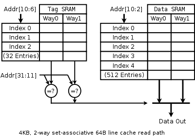 Read path for a 2-way associative cache
The diagram to the right is intended to clarify the manner in which the various fields of the address are used. Address bit 31 is most significant, bit 0 is least significant. The diagram shows the SRAMs, indexing, and multiplexing for a 4 kB, 2-way set-associative, virtually indexed and virtually tagged cache with 64 B lines, a 32b read width and 32b virtual address.
Because the cache is 4 kB and has 64 B lines, there are just 64 lines in the cache, and we read two at a time from a Tag SRAM which has 32 rows, each with a pair of 21 bit tags. Although any function of virtual address bits 31 through 6 could be used to index the tag and data SRAMs, it is simplest to use the least significant bits.
Similarly, because the cache is 4 kB and has a 4 B read path, and reads two ways for each access, the Data SRAM is 512 rows by 8 bytes wide.
A more modern cache might be 16 kB, 4-way set-associative, virtually indexed, virtually hinted, and physically tagged, with 32 B lines, 32b read width and 36b physical addresses. The read path recurrence for such a cache looks very similar to the path above. Instead of tags, vhints are read, and matched against a subset of the virtual address. Later on in the pipeline, the virtual address is translated into a physical address by the TLB, and the physical tag is read (just one, as the vhint supplies which way of the cache to read). Finally the physical address is compared to the physical tag to determine if a hit has occurred.
Some SPARC designs have improved the speed of their L1 caches by a few gate delays by collapsing the virtual address adder into the SRAM decoders. See Sum addressed decoder.
History
The early history of cache technology is closely tied to the invention and use of virtual memory.[citation needed] Because of scarcity and cost of semi-conductors memories, early mainframe computers in the 1960s used a complex hierarchy of physical memory, mapped onto a flat virtual memory space used by programs. The memory technologies would span semi-conductor, magnetic core, drum and disc. Virtual memory seen and used by programs would be flat and caching would be used to fetch data and instructions into the fastest memory ahead of processor access. Extensive studies were done to optimize the cache sizes. Optimal values were found to depend greatly on the programming language used with Algol needing the smallest and Fortran and Cobol needing the largest cache sizes.[disputed ]
In the early days of microcomputer technology, memory access was only slightly slower than register access. But since the 1980s [15] the performance gap between processor and memory has been growing. Microprocessors have advanced much faster than memory, especially in terms of their operating frequency, so memory became a performance bottleneck. While it was technically possible to have all the main memory as fast as the CPU, a more economically viable path has been taken: use plenty of low-speed memory, but also introduce a small high-speed cache memory to alleviate the performance gap. This provided an order of magnitude more capacity—for the same price—with only a slightly reduced combined performance.
First TLB implementations
The first documented uses of a TLB were on the GE 645[16] and the IBM 360/67,[17] both of which used an associative memory as a TLB.
First data cache
The first documented use of a data cache was on the IBM System/360 Model 85.[18]
In x86 microprocessors
As the x86 microprocessors reached clock rates of 20 MHz and above in the 386, small amounts of fast cache memory began to be featured in systems to improve performance. This was because the DRAM used for main memory had significant latency, up to 120 ns, as well as refresh cycles. The cache was constructed from more expensive, but significantly faster, SRAM, which at the time had latencies around 10 ns. The early caches were external to the processor and typically located on the motherboard in the form of eight or nine DIP devices placed in sockets to enable the cache as an optional extra or upgrade feature.
Some versions of the Intel 386 processor could support 16 to 64 kB of external cache.
With the 486 processor, an 8 kB cache was integrated directly into the CPU die. This cache was termed Level 1 or L1 cache to differentiate it from the slower on-motherboard, or Level 2 (L2) cache. These on-motherboard caches were much larger, with the most common size being 256 kB. The popularity of on-motherboard cache continued on through the Pentium MMX era but was made obsolete by the introduction of SDRAM and the growing disparity between bus clock rates and CPU clock rates, which caused on-motherboard cache to be only slightly faster than main memory.
The next evolution in cache implementation in the x86 microprocessors began with the Pentium Pro, which brought the secondary cache onto the same package as the microprocessor, clocked at the same frequency as the microprocessor.
On-motherboard caches enjoyed prolonged popularity thanks to the AMD K6-2 and AMD K6-III processors that still used the venerable Socket 7, which was previously used by Intel with on-motherboard caches. K6-III included 256 kb on-die L2 cache and took advantage of the on-board cache as a third level cache, named L3 (motherboards with up to 2 MB of on-board cache were produced). After the Socket-7 became obsolete, on-motherboard cache disappeared from the x86 systems.
The three-level cache was used again first with the introduction of multiple processor cores, where the L3 was added to the CPU die. It became common to have the three levels be larger in size than the next so that it became not uncommon to find Level 3 cache sizes of eight megabytes. This trend appears to continue for the foreseeable future.
Current research
Early cache designs focused entirely on the direct cost of cache and RAM and average execution speed. More recent cache designs also consider energy efficiency, fault tolerance, and other goals.[19]
There are several tools available to computer architects to help explore tradeoffs between cache cycle time, energy, and area. These tools include the open-source CACTI cache simulator[20] and the open-source SimpleScalar instruction set simulator.
See also
- Cache coherency
- Cache algorithms
- Dinero (Cache simulator by University of Wisconsin System)
- Instruction unit
- Memoization, briefly defined in List of computer term etymologies
- No-write allocation
- Scratchpad RAM
- Write buffer
Notes
References
- ^ TMS320C66x DSP Cache User Guide, Texas Instruments, November 2010, p. 1-5, http://www.ti.com/lit/ug/sprugy8/sprugy8.pdf
- ^ KDJ11-A CPU Module User's Guide, Educational Services of Digital Equipment Corporation, 1984, p. 1-27, http://bitsavers.org/pdf/dec/pdp11/1173/KDJ11-A_UsersManual.pdf
- ^ J.M. Tendler; J. S. Dodson; J. S. Fields, Jr.; H. Le; B. Sinharoy (January 2002), "POWER4 system microarchitecture", IBM Journal of Research & Development (International Business Machines Corporation) 46 (1): 15, doi:10.1147/rd.461.0005
- ^ http://ieeexplore.ieee.org/xpl/freeabs_all.jsp?arnumber=5234663
- ^ a b André Seznec. "A Case for Two-Way Skewed-Associative Caches". doi:10.1145/173682.165152.
- ^ a b "Advanced Caching Techniques" by C. Kozyrakis
- ^ Micro-Architecture "Skewed-associative caches have ... major advantages over conventional set-associative caches."
- ^ "Cache performance of SPEC CPU2000". Cs.wisc.edu. http://www.cs.wisc.edu/multifacet/misc/spec2000cache-data/. Retrieved 2010-05-02.
- ^ Sumner, F. H.; Haley, G.; Chenh, E. C. Y. (1962), "The Central Control Unit of the 'Atlas' Computer", Information Processing 1962, IFIP Congress Proceedings, Proceedings of IFIP Congress 62, Spartan.
- ^ Kilburn, T.; Payne, R. B.; Howarth, D. J. (December 1961), "The Atlas Supervisor", Computers - Key to Total Systems Control, Conferences Proceedings, 20 Proceedings of the Eastern Joint Computer Conference Washington, D.C., Macmillan, pp. 279–294, http://www.chilton-computing.org.uk/acl/technology/atlas/p019.htm.
- ^ "Understanding Caching". Linux Journal. http://www.linuxjournal.com/article/7105. Retrieved 2010-05-02.
- ^ http://www.systems.ethz.ch/education/courses/fs09/aos/lectures/wk3-print.pdf
- ^ "Trace Cache: a Low Latency Approach to High Bandwidth Instruction Fetching.". 1996. doi:10.1109/MICRO.1996.566447. http://citeseer.ist.psu.edu/viewdoc/summary?doi=10.1.1.140.2177.
- ^ "AMD K8". Sandpile.org. http://www.sandpile.org/impl/k8.htm. Retrieved 2007-06-02.
- ^ "The Processor-Memory performance gap". acm.org. http://www.acm.org/crossroads/xrds5-3/pmgap.html. Retrieved 2007-11-08.
- ^ GE (January 1968), GE-645 System Manual, http://bitsavers.org/pdf/ge/GE-645/GE-645_SystemMan_Jan68.pdf.
- ^ IBM (February, 1972), IBM System/360 Model 67 Functional Characteristics, Third Edition, GA27-2719-2, http://www.bitsavers.org/pdf/ibm/360/funcChar/GA27-2719-2_360-67_funcChar.pdf.
- ^ IBM (June, 1968), IBM System/360 Model 85 Functional Characteristics, SECOND EDITION, A22-6916-1, http://www.bitsavers.org/pdf/ibm/360/funcChar/A22-6916-1_360-85_funcChar_Jun68.pdf.
- ^ "Chip Design Thwarts Sneak Attack on Data" by Sally Adee 2009 discusses "A novel cache architecture with enhanced performance and security" [1] [2] by Zhenghong Wang and Ruby B. Lee: (abstract) "Caches ideally should have low miss rates and short access times, and should be power efficient at the same time. Such design goals are often contradictory in practice."
- ^ "CACTI". Hpl.hp.com. http://www.hpl.hp.com/research/cacti/. Retrieved 2010-05-02.
External links
- Memory part 2: CPU caches An article on lwn.net by Ulrich Drepper describing CPU caches in detail.
- Evaluating Associativity in CPU Caches — Hill and Smith — 1989 — Introduces capacity, conflict, and compulsory classification.
- Cache Performance for SPEC CPU2000 Benchmarks — Hill and Cantin — 2003 — This reference paper has been updated several times. It has thorough and lucidly presented simulation results for a reasonably wide set of benchmarks and cache organizations.
- Memory Hierarchy in Cache-Based Systems, by Ruud van der Pas, 2002, Sun Microsystems, is a nice introductory article to CPU memory caching.
- A Cache Primer by Paul Genua, P.E., 2004, Freescale Semiconductor, another introductory article.
- An 8-way set-associative cache written in VHDL
- Understanding CPU caching and performance An article on Ars Technica by Jon Stokes.
CPU technologies Architecture Parallelism PipelineLevelThreadsTypes Components Arithmetic logic unit (ALU) · Barrel shifter · Floating-point unit (FPU) · Back-side bus · Multiplexer · Demultiplexer · Registers · Memory management unit (MMU) · Translation lookaside buffer (TLB) · Cache · Register file · Microcode · Control unit · Clock ratePower management Categories:


Wikimedia Foundation. 2010.