- Intel 80486
Infobox Computer Hardware Cpu
name = Intel 486
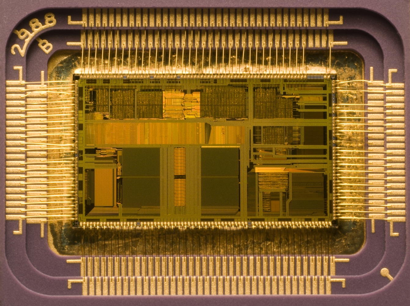
caption = The exposed die of an Intel 80486DX2 microprocessor.
manuf1 = Intel
manuf2 = IBM
produced-start = 1989
produced-end = 2007
size-from = 1, 0.8, 0.6
slowest = 16 | slow-unit = MHz
fastest = 100 | fast-unit = MHz
fsb-slowest = 16 | fsb-slow-unit = MHz
fsb-fastest = 50 | fsb-fast-unit = MHz
arch =x86
sock1 =Socket 1
sock2 =Socket 2
sock3 =Socket 3
numcores = 1The Intel 486, otherwise known as the 80486, i486 or just 486, was the first tightly pipelined
x86 design. Introduced in 1989, it was the first x86 chip that used more than a million transistors, due to a large on-chip cache and an integrated floating point unit. It represents a second generation of 32-bit x86 designs, following the original32-bit x86processor , theIntel 80386 , and a fourth generation ofbinary compatible CPUs since the 8086.(The i486 was so named, without the usual 80-prefix, because of a court ruling that prohibited trademarking numbers like 80486. Later, with the
Pentium , Intel dropped number-based naming altogether.)Improvements
The
instruction set of the i486 is very similar to its predecessor, theIntel 80386 , with the addition of only a few extra instructions, such as CMPXCHG which executes theCompare-and-swap atomic operation and the XADD which executes theFetch-and-add atomic operation. Though many atomic instructions have existed since the 8086/8088, they did not correspond to the atomic instructions implemented in certain RISC processors, which made it harder to port some applications from these processors.From a performance point of view, the architecture of the i486 is a vast improvement over the 80386. It has an on-chip unified instruction and data cache, an on-chip
floating-point unit (FPU), and an enhanced bus interface unit. In addition, simple instructions (such as ALU reg,reg) has a single clock throughput. These improvements yield a rough doubling in performance over the 386 at the sameclock rate . A 386 (or 286) chip therefore has to reach 50 MHz to be comparable with low end parts in the 486 series.Differences between the 386 and 486
* An 8 KiB on-chip SRAM
cache stores the most commonly used instructions and data (16 KiB and/or write-back on some later models). The 386 had no such internal cache but supported a slower off-chip cache.
* Tightly coupled pipelining allows the 486 to complete a simple instruction like ALU "reg,reg" or ALU "reg,im" every clock cycle. The 386 needed two clock cycles for this.
* Integrated FPU (disabled or absent in SX models) with a dedicated local bus gives faster floating point calculations compared to thei386 +i387 combination.
* Improved MMU performance.The 486 has a 32-bit
data bus and a 32-bitaddress bus . This required either four matched 30-pin (8-bit)SIMM s or one 72-pin (32-bit) SIMM on a typical PCmotherboard . The 32-bit address bus means that 4GiB of memory can be directly addressed.The Intel project manager for the 80486 was
Pat Gelsinger .In May 2006 Intel announced that production of the 80486 would cease at the end of September 2007. [http://www.reghardware.co.uk/2006/05/18/intel_cans_386_486_960_cpus/] Although the chip had long been obsolete for
personal computer applications, Intel had continued production for use inembedded systems . The 80486 was able to compute at up to 41 millioninstructions per second . [http://geocities.com/howcompworks/mp1.htm]Models
There are several suffixes and variants including:
*i486DX — The original chip (without any clock doubling).
*i486DX-S — SL Enhanced 486DX
*i486DXL — A 486DX with SMM (System Management Mode), stop clock, and power saving features.
*i486SX — an i486DX with the FPU part disabled or missing. Early variants were parts with disabled (defective) FPUs, later versions had the FPU removed from the die to reduce area and hence cost.
*i486SX-S — SL Enhanced 486SX
*i486SXL — A 486SX with SMM (System Management Mode), stop clock, and power saving features.
*i486DX2 — the internal processor clock runs at twice theclock rate of the external bus clock.
*i486SX2 — i486DX2 with the FPU disabled.
*i486SL — low power version of the i486DX, reduced VCore, power conservation circuitry - mainly for use in portable computers.
*i486SL-NM — i486SL based on i486SX
*i487SX — i486DX with a slightly different pinout sold as an FPU to i486SX systems; it was widely documented that i487SX when installed completely disabled the existing i486SX on themotherboard .
*i486 OverDrive — i486SX, i486SX2, i486DX2 or i486DX4. Marked as upgrade processors, some models had different pinouts or voltage handling abilities from 'standard' chips of the same speed stepping.
*i486DX4 — designed to run at triple clock rate (not quadruple as often believed; the DX3, which was meant to run at 2.5x the clock speed, was never released). DX4 models that featured write-back cache were identified by an "&EW" laser etched into their top surface, while the write-through models were identified by "&E".WT = Write-Through cache strategy, WB = Write-Back cache strategy
The specified maximum internal clock frequency (on Intels versions) ranged from 16 to 100 MHz. The 16MHz i486SX model was used by Dell Computers but sometimes ridiculed for the fact that it was handily beaten by many 386 systems. One of the few 486 models specified for a 50 MHz bus (486DX-50) initially had overheating problems and was moved to the 0.8 micrometre fabrication process. However, problems continued when installed in local bus systems due to the high bus speed, making it rather unpopular with mainstream consumers as local bus video was considered a requirement at the time. It was soon eclipsed by the clock-doubled i486DX2 which instead ran the CPU logic at twice the external bus speed. However, the 486DX-50 remained popular with users of EISA systems. More powerful 486 iterations such as the OverDrive and DX4 were less popular (the latter available as an OEM part only), as they came out after Intel had released the next generation
Pentium . Certain steppings of the DX4 also officially supported 50MHz bus operation but was a seldom used feature.Gaming
The 486DX2 66 MHz was the most widespread high-end 486 version. For many players of
video games during the early and mid 1990s, towards the end of theMS-DOS gaming era, it was often coupled with 8 - 16 MB RAM and a VLB video card. This configuration was capable of running every title available for several years after its release, making it a "sweet spot " in CPU performance and longevity. The introduction of3D computer graphics spelled the end of the 486's reign, because of its heavy use offloating point calculations and the need for fasterCPU cache and morememory bandwidth . Developers also began to target the Pentium almost exclusively withx86 assembly language optimizations (e.g.Quake ).Competitive alternatives
486 compatible processors have been produced by other companies such as IBM,
Texas Instruments ,AMD ,Cyrix , UMC, andSGS Thompson . Some are near duplicates in terms of specifications and performance, some are not. The 486 was, however, covered by many of Intel's 386 patents as well as some of its own. Intel and IBM have broad cross-licenses of these patents, and AMD was granted rights to the relevant patents in the 1995 settlement of a lawsuit between the companies. [http://www.amd.com/us-en/assets/content_type/DownloadableAssets/AMD_-_Intel_Litigation_History.pdf]AMD produced several models of the 486 using the 40MHz bus (486DX-40, 486DX/2-80 & 486DX/4-120) not available from Intel, as well a 90MHz part using a proprietary 30MHz for OEM use only. The fastest running 486 CPU, the
Am5x86 ,ran at 133MHz was released by AMD in 1995. 150MHz and 160MHz parts were planned but never officially released.Motherboards and Buses
Early 486 machines were equipped with several ISA (Industry Standard Architecture) aka "AT-Bus" slots and sometimes one or two
8-bit -only "PC/XT-Bus" slots. Manymotherboard s enabled overclocking of these up from the default 6 or 8 MHz to perhaps 16.5 or 20 MHz (half the i486 bus clock) in a number of steps, often from within theBIOS setup. Especially older peripheral cards normally worked well at such speeds as they often used standard MSI chips instead of slower (at the time) custom VLSI designs. This could give significant performance gains (such as for old video cards moved from a 386 or 286 computer, for example). However, operation beyond 8 or 10MHz could lead to stability problems, particularly in systems equipped with SCSI and/or sound cards.Some motherboards came equipped with a 32-bit version of the ISA-standard called EISA (Extended Industry Standard Architecture), and offered a number of attractive features such as increased bandwidth, extended addressing and IRQ sharing. However, EISA cards were very expensive and later relegated to the server and workstation arena, being rather quickly supplanted by the simpler but faster (and often buggy) VLB (VESA Local Bus) on consumer desktops. PCI (Peripheral Component Interconnect) then began gradually replacing VLB during the final one or two years of the 486's sale life.
Mature 486 boards were normally equipped with both PCI- and ISA-slots, and sometimes a single VLB-slot as well. In this configuration VLB or PCI though-put sometimes suffered greatly depending on how the buses were bridged. In this setup the VL-Bus slot was usually only compatible with video cards (VLB-IDE, multi I/O, or SCSI cards often had problems on motherboards with PCI slots). The VL-Bus operated at the same clock speed as the i486-bus (basically "being" a local 486-bus). The PCI bus also usually depended on the i486 clock but sometimes had a divider setting available via the BIOS. This could be set to 1/1 or 1/2, sometimes even 2/3 (for 50MHz CPU clocks). Some boards limited the PCI clock to the specified maximum of 33 MHz (certain network cards assumed 33MHz and would produce erroneous bit-rates in an overclocked slot). The ISA clock was either generated by a separate clock generator or by a divider of the VLB/PCI clock.
One of the earliest complete systems to use the 80486 chip was the Apricot VX FT, produced by United Kingdom hardware manufacturer
Apricot Computers . Even overseas in the United States it drew attention as "The World's First 486" in a popular September 1989 issue of "Byte" magazine (shown right).Later 486 boards also supported
Plug-And-Play , theMicrosoft technology that began as a part ofWindows 95 designed to make component installation easier for consumers.Obsolescense
Windows 95 signaled the end of the 486 era due to its high memory requirements (16MB to perform as well as Windows 3.x with just 8MB). Many 486 users at that time were running eight 1MB 30-pin SIMMs leaving no available slots for expansion. As 4meg 30-pin SIMMs were still very expensive at that time, it made more sense to buy a Pentium rather than spend a premium on upgrading a system that was nearing the end of its service life. The 486 were used as budget machine for people who could not afford the latest computers until around 2001 when Windows 95 was not supported and Windows 98, ME, NT 4.0, 2000, NT 4.0 and XP required more powerful computers.References
ee also
*
List of Intel microprocessors
*Motorola 68040 , although not compatible, often positioned as theMotorola equivalent to the Intel 80486 in terms of performance and features.
* [http://www.mindshare.com/addtech/486%20Book.pdf "80486 System Architecture" published by Mindshare (pdf)]Notes
External links
* [http://www.cpu-collection.de/?l0=co&l1=Intel&l2=i486%20DX Intel 80486 images and descriptions at cpu-collection.de]
* [http://www.cpu-info.com/index2.php?mainid=html/cpu/486.php CPU-INFO: 80486, indepth processor history]
Wikimedia Foundation. 2010.