- Classic RISC pipeline
-
In the history of computer hardware, some early reduced instruction set computer central processing units (RISC CPUs) used a very similar architectural solution, now called a classic RISC pipeline. Those CPUs were: MIPS, SPARC, Motorola 88000, and later DLX.
Each of these classic scalar RISC designs fetched and attempted to execute one instruction per cycle. The main common concept of each design was a five stage execution instruction pipeline. During operation, each pipeline stage would work on one instruction at a time.
Each of these stages consisted of an initial set of flip-flops, and combinational logic which operated on the outputs of those flops.
Contents
The classic five stage RISC pipeline
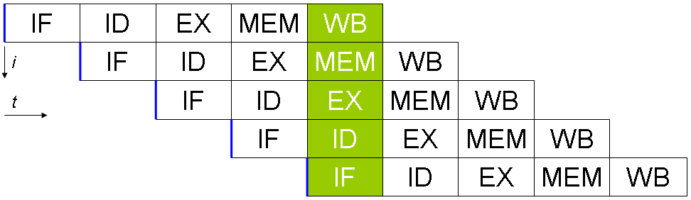
 Basic five-stage pipeline in a RISC machine (IF = Instruction Fetch, ID = Instruction Decode, EX = Execute, MEM = Memory access, WB = Register write back). The vertical axis is successive instructions; the horizontal axis is time. So in the green column, the earliest instruction is in WB stage, and the latest instruction is undergoing instruction fetch.
Instruction fetch
The Instruction Cache on these machines had a latency of one cycle. During the Instruction Fetch stage, a 32-bit instruction was fetched from the cache.
The PC predictor sends the Program Counter (PC) to the Instruction Cache to read the current instruction. At the same time, the PC predictor predicts the address of the next instruction by incrementing the PC by 4 (all instructions were 4 bytes long). This prediction was always wrong in the case of a taken branch, jump, or exception (see delayed branches, below). Later machines would use more complicated and accurate algorithms (branch prediction and branch target prediction) to guess the next instruction address.
Decode
Unlike earlier microcoded machines, the first RISC machines had no microcode. Once fetched from the instruction cache, the instruction bits were shifted down the pipeline, so that simple combinational logic in each pipeline stage could produce the control signals for the datapath directly from the instruction bits. As a result, very little decoding is done in the stage traditionally called the decode stage.
All MIPS, SPARC, and DLX instructions have at most two register inputs. During the decode stage, these two register names are identified within the instruction, and the two registers named are read from the register file. In the MIPS design, the register file had 32 entries.
At the same time the register file was read, instruction issue logic in this stage determined if the pipeline was ready to execute the instruction in this stage. If not, the issue logic would cause both the Instruction Fetch stage and the Decode stage to stall. On a stall cycle, the stages would prevent their initial flops from accepting new bits.
If the instruction decoded was a branch or jump, the target address of the branch or jump was computed in parallel with reading the register file. The branch condition is computed after the register file is read, and if the branch is taken or if the instruction is a jump, the PC predictor in the first stage is assigned the branch target, rather than the incremented PC that has been computed.
The decode stage ended up with quite a lot of hardware: the MIPS instruction set had the possibility of branching if two registers were equal, so a 32-bit-wide AND tree ran in series after the register file read, making a very long critical path through this stage. Also, the branch target computation generally required a 16 bit add and a 14 bit incrementer. Resolving the branch in the decode stage made it possible to have just a single-cycle branch mispredict penalty. Since branches were very often taken (and thus mispredicted), it was very important to keep this penalty low.
Execute
Instructions on these simple RISC machines can be divided into three latency classes according to the type of the operation:
- Register-Register Operation (Single cycle latency): Add, subtract, compare, and logical operations. During the execute stage, the two arguments were fed to a simple ALU, which generated the result by the end of the execute stage.
- Memory Reference (Two cycle latency). All loads from memory. During the execute stage, the ALU added the two arguments (a register and a constant offset) to produce a virtual address by the end of the cycle.
- Multi Cycle Instructions (Many cycle latency). Integer multiply and divide and all floating-point operations. During the execute stage, the operands to these operations were fed to the multi-cycle multiply/divide unit. The rest of the pipeline was free to continue execution while the multiply/divide unit did its work. To avoid complicating the writeback stage and issue logic, multicycle instruction wrote their results to a separate set of registers.
Memory Access
During this stage, single cycle latency instructions simply have their results forwarded to the next stage. This forwarding ensures that both single and two cycle instructions always write their results in the same stage of the pipeline, so that just one write port to the register file can be used, and it is always available.
If the instruction is a load, the data is read from the data cache, as follows:
There have been a wide variety of data cache organizations. By far the simplest is direct mapped and virtually tagged, which is what will be assumed for the following explanation.
The cache has two SRAMs (Static RAM), one storing data, the other storing tags. During a load, the SRAMs are read in parallel during the access stage. The single tag read is compared with the virtual address specified by the load.
If the two are equal, then the datum we are looking for is resident in the cache, and has just been read from the data SRAM. The load is a hit, and the load instruction can complete the writeback stage normally.
If the tag and virtual address are not equal, then the line is not in the cache. The CPU pipeline must suspend operation (described below under Cache Miss Handling) while a state machine reads the required data from memory into the cache, and optionally writes any dirty data evicted from the cache back into memory.
During a store, the tag SRAM is read to determine if the store is a hit or miss, and if a miss, the same state machine brings the datum into the cache. Store data cannot be written to the cache data SRAM during the access stage because the processor does not yet know if the correct line is resident. Instead, the store data is held in a Store Data Queue, until it can be written to the cache data SRAM during the next store instruction. In a classic RISC pipeline, the Store Data Queue is just a single 32 bit register. For later reference, the virtual address written is held in the Store Address Queue, again just a single 32 bit register. On more complicated pipelines, these queues actually have multiple hardware registers and variable length.
There is one more complication. A load immediately after a store could reference the same memory address, in which case the data must come from the Store Data Queue rather than from the cache's data SRAM. So, during a load, the load address is also checked against the Store Address Queue. If there is a match, the data from the Store Data Queue is forwarded to the writeback stage, rather than the data from the data SRAM. This operation does not change the flow of the load operation through the pipeline.
Writeback
During this stage, both single cycle and two cycle instructions write their results into the register file.
Hazards
Hennessy and Patterson coined the term hazard for situations in which a completely trivial pipeline would produce wrong answers.
Structural Hazards
Structural hazards are when two instructions might attempt to use the same resources at the same time. Classic RISC pipelines avoided these hazards by replicating hardware. In particular, branch instructions could have used the ALU to compute the target address of the branch. If the ALU were used in the decode stage for that purpose, an ALU instruction followed by a branch would have seen both instructions attempt to use the ALU simultaneously. It is simple to resolve this conflict by designing a specialized branch target adder into the decode stage.
Data Hazards
Data hazards are when an instruction, scheduled blindly, would attempt to use data before the data is available in the register file.
Data hazards are avoided in one of two ways:
Solution A. Bypassing
Suppose the CPU is executing the following piece of code:
SUB r3,r4 -> r10    ; Writes r3-r4 to r10
AND r10,3 -> r11    ; Writes r10 & 3 to r11
The instruction fetch and decode stages will send the second instruction one cycle after the first. They flow down the pipeline as shown in this diagram:
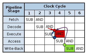
In a naïve pipeline, without hazard consideration, the data hazard progresses as follows:
In cycle 3, the SUB instruction calculates the new value for r10. In the same cycle, the AND operation is decoded, and the value of r10 is fetched from the register file. However, the SUB instruction has not yet written its result to r10. Write-back of this normally occurs in cycle 5 (green box). Therefore, the value read from the register file and passed to the ALU (in the Execute stage of the AND operation, red box) is incorrect.
Instead, we must pass the data that was computed by SUB back to the Execute stage (i.e. to the red circle in the diagram) of the AND operation before it is normally written-back. The solution to this problem is a pair of bypass multiplexers. These multiplexers sit at the end of the decode stage, and their flopped outputs are the inputs to the ALU. Each multiplexer selects between:
- A register file read port (i.e. the output of the decode stage, as in the naïve pipeline): red arrow
- The current register pipeline of the ALU (to bypass by one stage): blue arrow
- The current register pipeline of the access stage (which is either a loaded value or a forwarded ALU result, this provides bypassing of two stages): purple arrow. Note that this requires the data to be passed backwards in time by one cycle. If this occurs, a bubble must be inserted to stall the AND operation until the data is ready.
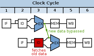
Decode stage logic compares the registers written by instructions in the execute and access stages of the pipeline to the registers read by the instruction in the decode stage, and cause the multiplexers to select the most recent data. These bypass multiplexers make it possible for the pipeline to execute simple instructions with just the latency of the ALU, the multiplexer, and a flip-flop. Without the multiplexers, the latency of writing and then reading the register file would have to be included in the latency of these instructions.
Note that the data can only be passed forward in time - the data cannot be bypassed back to an earlier stage if it has not be processed yet. In the case above, the data is passed forward (by the time the AND is ready for the register in the ALU, the SUB has already computed it).
Solution B. Pipeline Interlock
However, consider the following instructions:
LD  adr    -> r10
AND r10, 3 -> r11
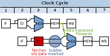
The data read from the address adr will not be present in the data cache until after the Memory Access stage of the LDB instruction. By this time, the AND instruction will already be through the ALU. To resolve this would require the data from memory to be passed backwards in time to the input to the ALU. This is not possible. The solution is to delay the AND instruction by one cycle. The data hazard is detected in the decode stage, and the fetch and decode stages are stalled - they are prevented from flopping their inputs and so stay in the same state for a cycle. The execute, access, and write-back stages downstream see an extra no-operation instruction (NOP) inserted between the LD and AND instructions.
This NOP is termed a "pipeline bubble" since it floats in the pipeline, like an air bubble, occupying resources but not producing useful results. The hardware to detect a data hazard and stall the pipeline until the hazard is cleared is called a pipeline interlock.
Bypassing backwards in time Problem resolved using a bubble 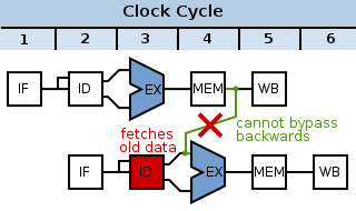
A pipeline interlock does not have to be used with any data forwarding, however. The first example of the SUB followed by AND and the second example of LD followed by AND can be solved by stalling the first stage by three cycles until write-back is achieved, and the data in the register file is correct, causing the correct register value to be fetched by the AND's Decode stage. This causes quite a performance hit, as the processor spends a lot of time processing nothing, but clock speeds can be increased as there is less forwarding logic to wait for.
This data hazard can be detected quite easily when the program's machine code is written by the compiler. The original Stanford RISC machine relied on the compiler to add the NOP instructions in this case, rather than having the circuitry to detect and (more taxingly) stall the first two pipeline stages. Hence the name MIPS: Microprocessor without Interlocked Pipeline Stages. It turned out that the extra NOP instructions added by the compiler expanded the program binaries enough that the instruction cache hit rate was reduced. The stall hardware, although expensive, was put back into later designs to improve instruction cache hit rate, at which point the acronym no longer made sense.
Control Hazards
Control hazards are caused by conditional and unconditional branching. The classic RISC pipeline resolves branches in the Decode stage, which means the branch resolution recurrence is two cycles long. There are three implications:
- The branch resolution recurrence goes through quite a bit of circuitry: the instruction cache read, register file read, branch condition compute (which involves a 32 bit compare on the MIPS CPUs), and the next instruction address multiplexer.
- Because branch and jump targets are calculated in parallel to the register read, RISC ISAs typically do not have instructions which branch to a register+offset address. Jump to register is supported.
- On any branch taken, the instruction immediately after the branch is always fetched from the instruction cache. If this instruction is ignored, there is a one cycle per taken branch IPC penalty, which is quite large.
There are four schemes to solve this performance problem with branches:
- Predict Not Taken: Always fetch the instruction after the branch from the instruction cache, but only execute it if the branch is not taken. If the branch is not taken, the pipeline stays full. If the branch is taken, the instruction is flushed (marked as if it were a NOP), and we lose 1 cycle's opportunity to finish an instruction.
- Branch Likely: Always fetch the instruction after the branch from the instruction cache, but only execute it if the branch was taken. The compiler can always fill the branch delay slot on such a branch, and since branches are more often taken than not, such branches have a smaller IPC penalty than the previous kind.
- Branch Delay Slot: Always fetch the instruction after the branch from the instruction cache, and always execute it, even if the branch is taken. Instead of taking an IPC penalty for some fraction of branches either taken (perhaps 60%) or not taken (perhaps 40%), branch delay slots take an IPC penalty for the those branches into which the compiler could not schedule the branch delay slot. The SPARC, MIPS, and MC88K designers designed a Branch delay slot into their ISAs.
- Branch Prediction: In parallel with fetching each instruction, guess if the instruction is a branch or jump, and if so, guess the target. On the cycle after a branch or jump, fetch the instruction at the guessed target. When the guess is wrong, flush the incorrectly fetched target.
Delayed branches were controversial, first, because their semantics are complicated. A delayed branch specifies that the jump to a new location happens after the next instruction. That next instruction is the one unavoidably loaded by the instruction cache after the branch.
Delayed branches have been criticized as a poor short-term choice in ISA design:
- Compilers typically have some difficulty finding logically independent instructions to place after the branch (the instruction after the branch is called the delay slot), so that they must insert NOPs into the delay slots.
- Superscalar processors, which fetch multiple instructions per cycle and must have some form of branch prediction, do not benefit from delayed branches. The Alpha ISA left out delayed branches, as it was intended for superscalar processors.
- The most serious drawback to delayed branches is the additional control complexity they entail. If the delay slot instruction takes an exception, the processor has to be restarted on the branch, rather than that next instruction. Exceptions now have essentially two addresses, the exception address and the restart address, and generating and distinguishing between the two correctly in all cases has been a source of bugs for later designs.
Exceptions
Suppose a 32-bit RISC is processing an ADD instruction which adds two large numbers together. Suppose the resulting number does not fit in 32 bits. What happens?
The simplest solution, provided by every architecture, is wrapping arithmetic. This is the standard arithmetic provided by the language C. Numbers greater than the maximum possible encoded value have their most significant bits chopped off until they fit. In the usual integer number system, 3000000000+3000000000=6000000000. With unsigned 32 bit wrapping arithmetic, 3000000000+3000000000=1705032704 (6000000000 mod 2^32). This may not seem terribly useful. The largest benefit of wrapping arithmetic is that every operation has a well defined result.
But the programmer, especially if programming in a language supporting large integers (e.g. Lisp or Scheme), may not want wrapping arithmetic. Some architectures (e.g. MIPS), define special addition operations that branch to special locations on overflow, rather than wrapping the result. Software at the target location is responsible for fixing the problem. This special branch is called an exception. Exceptions differ from regular branches in that the target address is not specified by the instruction itself, and the branch decision is dependent on the outcome of the instruction.
The most common kind of software-visible exception on one of the classic RISC machines is a TLB miss (see virtual memory).
Exceptions are different from branches and jumps, because those other control flow changes are resolved in the decode stage. Exceptions are resolved in the writeback stage. When an exception is detected, the following instructions (earlier in the pipeline) are marked as invalid, and as they flow to the end of the pipe their results are discarded. The program counter is set to the address of a special exception handler, and special registers are written with the exception location and cause.
To make it easy (and fast) for the software to fix the problem and restart the program, the CPU must take a precise exception. A precise exception means that all instructions up to the excepting instruction have been executed, and the excepting instruction and everything afterwards have not been executed.
In order to take precise exceptions, the CPU must commit changes to the software visible state in the program order. This in-order commit happens very naturally in the classic RISC pipeline. Most instructions write their results to the register file in the writeback stage, and so those writes automatically happen in program order. Store instructions, however, write their results to the Store Data Queue in the access stage. If the store instruction takes an exception, the Store Data Queue entry is invalidated so that it is not written to the cache data SRAM later.
Cache miss handling
Occasionally, either the data or instruction cache will not have a datum or instruction required. In these cases, the CPU must suspend operation until the cache can be filled with the necessary data, and then must resume execution. The problem of filling the cache with the required data (and potentially writing back to memory the evicted cache line) is not specific to the pipeline organization, and is not discussed here.
There are two strategies to handle the suspend/resume problem. The first is a global stall signal. This signal, when activated, prevents instructions from advancing down the pipeline, generally by gating off the clock to the flip-flops at the start of each stage. The disadvantage of this strategy is that there are a large number of flip flops, so the global stall signal takes a long time to propagate. Since the machine generally has to stall in the same cycle that it identifies the condition requiring the stall, the stall signal becomes a speed-limiting critical path.
Another strategy to handle suspend/resume is to reuse the exception logic. The machine takes an exception on the offending instruction, and all further instructions are invalidated. When the cache has been filled with the necessary data, the instruction which caused the cache miss is restarted. To expedite data cache miss handling, the instruction can be restarted so that its access cycle happens one cycle after the data cache has been filled.
Categories:- Instruction processing


Wikimedia Foundation. 2010.