- Laser diode
-

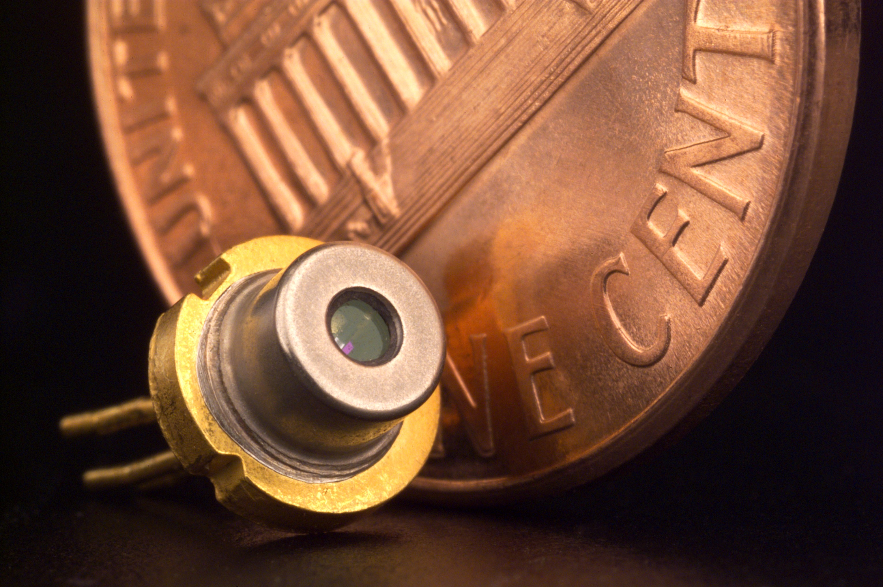
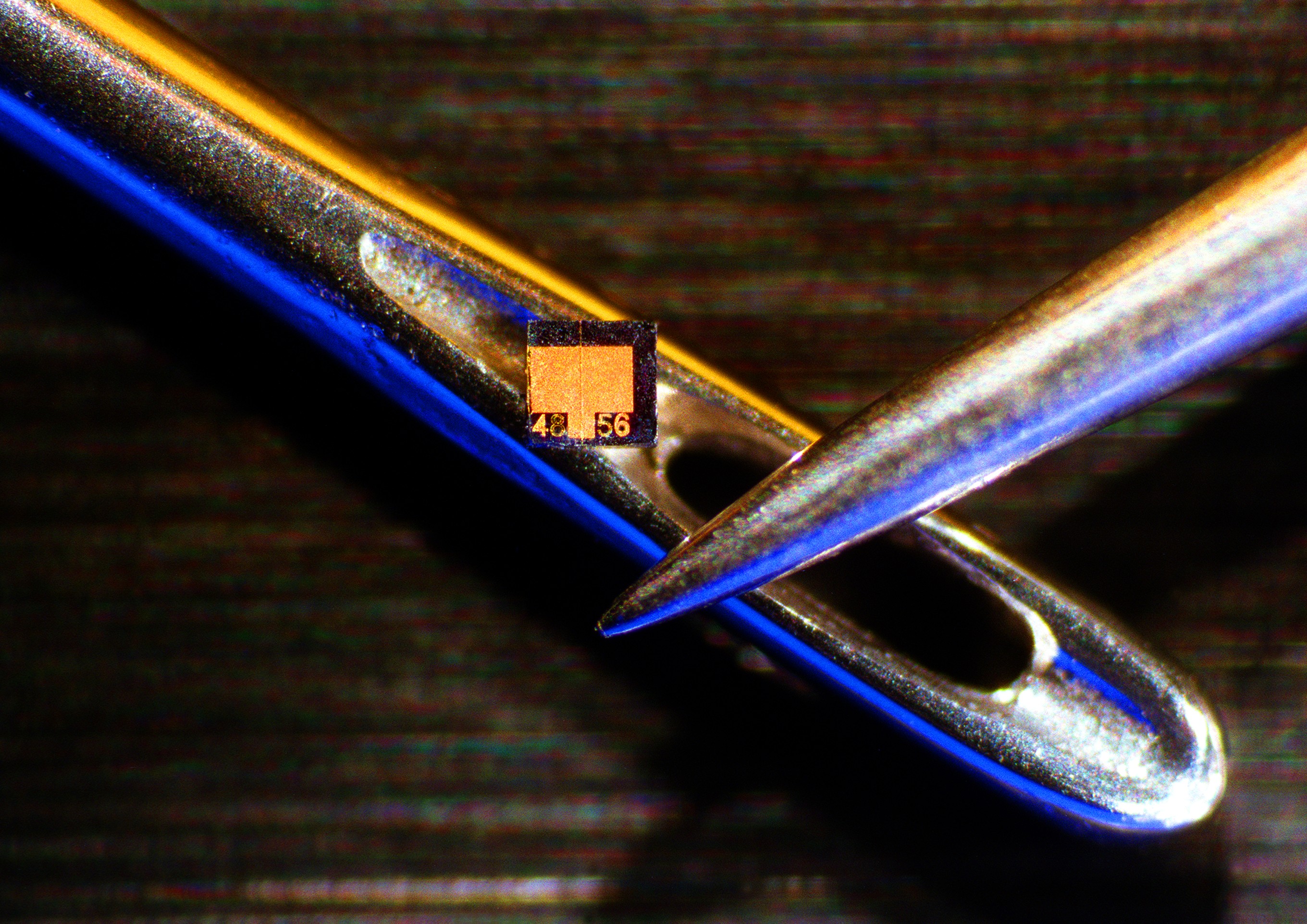
 Top: a packaged laser diode shown with a penny for scale. Bottom: the laser diode chip is removed from the above package and placed on the eye of a needle for scale.
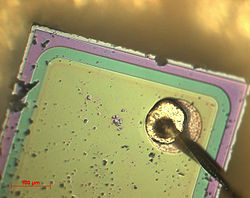 A visible light micrograph of a laser diode taken from a CD-ROM drive. Visible are the P and N layers distinguished by different colours, and scattered glass fragments from a broken collimator lens.
The laser diode is a laser where the active medium is a semiconductor similar to that found in a light-emitting diode. The most common type of laser diode is formed from a p-n junction and powered by injected electric current. The former devices are sometimes referred to as injection laser diodes to distinguish them from optically pumped laser diodes.
Contents
Theory of operation
A laser diode is formed by doping a very thin layer on the surface of a crystal wafer. The crystal is doped to produce an n-type region and a p-type region, one above the other, resulting in a p-n junction, or diode.
Laser diodes form a subset of the larger classification of semiconductor p-n junction diodes. Forward electrical bias across the laser diode causes the two species of charge carrier – holes and electrons – to be "injected" from opposite sides of the p-n junction into the depletion region. Holes are injected from the p-doped, and electrons from the n-doped, semiconductor. (A depletion region, devoid of any charge carriers, forms as a result of the difference in electrical potential between n- and p-type semiconductors wherever they are in physical contact.) Due to the use of charge injection in powering most diode lasers, this class of lasers is sometimes termed "injection lasers," or "injection laser diode" (ILD). As diode lasers are semiconductor devices, they may also be classified as semiconductor lasers. Either designation distinguishes diode lasers from solid-state lasers.
Another method of powering some diode lasers is the use of optical pumping. Optically Pumped Semiconductor Lasers (OPSL) use a III-V semiconductor chip as the gain media, and another laser (often another diode laser) as the pump source. OPSL offer several advantages over ILDs, particularly in wavelength selection and lack of interference from internal electrode structures.[1][2]
When an electron and a hole are present in the same region, they may recombine or "annihilate" with the result being spontaneous emission — i.e., the electron may re-occupy the energy state of the hole, emitting a photon with energy equal to the difference between the electron and hole states involved. (In a conventional semiconductor junction diode, the energy released from the recombination of electrons and holes is carried away as phonons, i.e., lattice vibrations, rather than as photons.) Spontaneous emission gives the laser diode below lasing threshold similar properties to an LED. Spontaneous emission is necessary to initiate laser oscillation, but it is one among several sources of inefficiency once the laser is oscillating.
The difference between the photon-emitting semiconductor laser and conventional phonon-emitting (non-light-emitting) semiconductor junction diodes lies in the use of a different type of semiconductor, one whose physical and atomic structure confers the possibility for photon emission. These photon-emitting semiconductors are the so-called "direct bandgap" semiconductors. The properties of silicon and germanium, which are single-element semiconductors, have bandgaps that do not align in the way needed to allow photon emission and are not considered "direct." Other materials, the so-called compound semiconductors, have virtually identical crystalline structures as silicon or germanium but use alternating arrangements of two different atomic species in a checkerboard-like pattern to break the symmetry. The transition between the materials in the alternating pattern creates the critical "direct bandgap" property. Gallium arsenide, indium phosphide, gallium antimonide, and gallium nitride are all examples of compound semiconductor materials that can be used to create junction diodes that emit light.
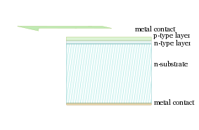 Diagram of a simple laser diode, such as shown above; not to scale
In the absence of stimulated emission (e.g., lasing) conditions, electrons and holes may coexist in proximity to one another, without recombining, for a certain time, termed the "upper-state lifetime" or "recombination time" (about a nanosecond for typical diode laser materials), before they recombine. Then a nearby photon with energy equal to the recombination energy can cause recombination by stimulated emission. This generates another photon of the same frequency, travelling in the same direction, with the same polarization and phase as the first photon. This means that stimulated emission causes gain in an optical wave (of the correct wavelength) in the injection region, and the gain increases as the number of electrons and holes injected across the junction increases. The spontaneous and stimulated emission processes are vastly more efficient in direct bandgap semiconductors than in indirect bandgap semiconductors; therefore silicon is not a common material for laser diodes.
As in other lasers, the gain region is surrounded with an optical cavity to form a laser. In the simplest form of laser diode, an optical waveguide is made on that crystal surface, such that the light is confined to a relatively narrow line. The two ends of the crystal are cleaved to form perfectly smooth, parallel edges, forming a Fabry–Pérot resonator. Photons emitted into a mode of the waveguide will travel along the waveguide and be reflected several times from each end face before they are emitted. As a light wave passes through the cavity, it is amplified by stimulated emission, but light is also lost due to absorption and by incomplete reflection from the end facets. Finally, if there is more amplification than loss, the diode begins to "lase".
Some important properties of laser diodes are determined by the geometry of the optical cavity. Generally, in the vertical direction, the light is contained in a very thin layer, and the structure supports only a single optical mode in the direction perpendicular to the layers. In the transverse direction, if the waveguide is wide compared to the wavelength of light, then the waveguide can support multiple transverse optical modes, and the laser is known as "multi-mode". These transversely multi-mode lasers are adequate in cases where one needs a very large amount of power, but not a small diffraction-limited beam; for example in printing, activating chemicals, or pumping other types of lasers.
In applications where a small focused beam is needed, the waveguide must be made narrow, on the order of the optical wavelength. This way, only a single transverse mode is supported and one ends up with a diffraction-limited beam. Such single spatial mode devices are used for optical storage, laser pointers, and fiber optics. Note that these lasers may still support multiple longitudinal modes, and thus can lase at multiple wavelengths simultaneously.
The wavelength emitted is a function of the band-gap of the semiconductor and the modes of the optical cavity. In general, the maximum gain will occur for photons with energy slightly above the band-gap energy, and the modes nearest the gain peak will lase most strongly. If the diode is driven strongly enough, additional side modes may also lase. Some laser diodes, such as most visible lasers, operate at a single wavelength, but that wavelength is unstable and changes due to fluctuations in current or temperature.
Due to diffraction, the beam diverges (expands) rapidly after leaving the chip, typically at 30 degrees vertically by 10 degrees laterally. A lens must be used in order to form a collimated beam like that produced by a laser pointer. If a circular beam is required, cylindrical lenses and other optics are used. For single spatial mode lasers, using symmetrical lenses, the collimated beam ends up being elliptical in shape, due to the difference in the vertical and lateral divergences. This is easily observable with a red laser pointer.
The simple diode described above has been heavily modified in recent years to accommodate modern technology, resulting in a variety of types of laser diodes, as described below.
Types
The simple laser diode structure, described above, is extremely inefficient. Such devices require so much power that they can only achieve pulsed operation without damage. Although historically important and easy to explain, such devices are not practical.
Double heterostructure lasers
 Diagram of front view of a double heterostructure laser diode; not to scale
In these devices, a layer of low bandgap material is sandwiched between two high bandgap layers. One commonly-used pair of materials is gallium arsenide (GaAs) with aluminium gallium arsenide (AlxGa(1-x)As). Each of the junctions between different bandgap materials is called a heterostructure, hence the name "double heterostructure laser" or DH laser. The kind of laser diode described in the first part of the article may be referred to as a homojunction laser, for contrast with these more popular devices.
The advantage of a DH laser is that the region where free electrons and holes exist simultaneously—the active region—is confined to the thin middle layer. This means that many more of the electron-hole pairs can contribute to amplification—not so many are left out in the poorly amplifying periphery. In addition, light is reflected from the heterojunction; hence, the light is confined to the region where the amplification takes place.
Quantum well lasers
Main article: Quantum well laser Diagram of front view of a simple quantum well laser diode; not to scale
If the middle layer is made thin enough, it acts as a quantum well. This means that the vertical variation of the electron's wavefunction, and thus a component of its energy, is quantized. The efficiency of a quantum well laser is greater than that of a bulk laser because the density of states function of electrons in the quantum well system has an abrupt edge that concentrates electrons in energy states that contribute to laser action.
Lasers containing more than one quantum well layer are known as multiple quantum well lasers. Multiple quantum wells improve the overlap of the gain region with the optical waveguide mode.
Further improvements in the laser efficiency have also been demonstrated by reducing the quantum well layer to a quantum wire or to a "sea" of quantum dots.
Quantum cascade lasers
Main article: Quantum cascade laserIn a quantum cascade laser, the difference between quantum well energy levels is used for the laser transition instead of the bandgap. This enables laser action at relatively long wavelengths, which can be tuned simply by altering the thickness of the layer. They are heterojunction lasers.
Separate confinement heterostructure lasers
 Diagram of front view of a separate confinement heterostructure quantum well laser diode; not to scale
The problem with the simple quantum well diode described above is that the thin layer is simply too small to effectively confine the light. To compensate, another two layers are added on, outside the first three. These layers have a lower refractive index than the centre layers, and hence confine the light effectively. Such a design is called a separate confinement heterostructure (SCH) laser diode.
Almost all commercial laser diodes since the 1990s have been SCH quantum well diodes.
Distributed feedback lasers
Main article: Distributed feedback laserDistributed feedback lasers (DFB) are the most common transmitter type in DWDM-systems. To stabilize the lasing wavelength, a diffraction grating is etched close to the p-n junction of the diode. This grating acts like an optical filter, causing a single wavelength to be fed back to the gain region and lase. Since the grating provides the feedback that is required for lasing, reflection from the facets is not required. Thus, at least one facet of a DFB is anti-reflection coated. The DFB laser has a stable wavelength that is set during manufacturing by the pitch of the grating, and can only be tuned slightly with temperature. DFB lasers are widely used in optical communication applications where a precise and stable wavelength is critical.
The threshold current of this DFB laser, based on its static characteristic, is around 11 mA. The appropriate bias current in a linear regime could be taken in the middle of the static characteristic (50 mA).
VCSELs
Main article: Vertical-cavity surface-emitting laser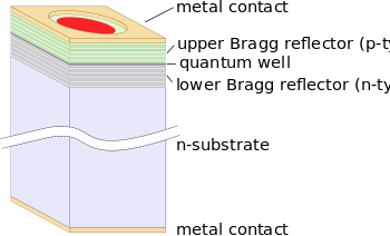 Diagram of a simple VCSEL structure; not to scale
Vertical-cavity surface-emitting lasers (VCSELs) have the optical cavity axis along the direction of current flow rather than perpendicular to the current flow as in conventional laser diodes. The active region length is very short compared with the lateral dimensions so that the radiation emerges from the surface of the cavity rather than from its edge as shown in the figure. The reflectors at the ends of the cavity are dielectric mirrors made from alternating high and low refractive index quarter-wave thick multilayer.
Such dielectric mirrors provide a high degree of wavelength-selective reflectance at the required free surface wavelength λ if the thicknesses of alternating layers d1 and d2 with refractive indices n1 and n2 are such that n1d1 + n2d2 = λ/2 which then leads to the constructive interference of all partially reflected waves at the interfaces. But there is a disadvantage: because of the high mirror reflectivities, VCSELs have lower output powers when compared to edge-emitting lasers.
There are several advantages to producing VCSELs when compared with the production process of edge-emitting lasers. Edge-emitters cannot be tested until the end of the production process. If the edge-emitter does not work, whether due to bad contacts or poor material growth quality, the production time and the processing materials have been wasted. Additionally, because VCSELs emit the beam perpendicular to the active region of the laser as opposed to parallel as with an edge emitter, tens of thousands of VCSELs can be processed simultaneously on a three inch Gallium Arsenide wafer. Furthermore, even though the VCSEL production process is more labor and material intensive, the yield can be controlled to a more predictable outcome. However, they normally show a lower power output level.
VECSELs
Main article: Vertical-external-cavity surface-emitting-laserVertical external-cavity surface-emitting lasers, or VECSELs, are similar to VCSELs. In VCSELs, the mirrors are typically grown epitaxially as part of the diode structure, or grown separately and bonded directly to the semiconductor containing the active region. VECSELs are distinguished by a construction in which one of the two mirrors is external to the diode structure. As a result, the cavity includes a free-space region. A typical distance from the diode to the external mirror would be 1 cm.
One of the most interesting features of any VECSEL is the small thickness of the semiconductor gain region in the direction of propagation, less than 100 nm. In contrast, a conventional in-plane semiconductor laser entails light propagation over distances of from 250 µm upward to 2 mm or longer. The significance of the short propagation distance is that it causes the effect of "antiguiding" nonlinearities in the diode laser gain region to be minimized. The result is a large-cross-section single-mode optical beam which is not attainable from in-plane ("edge-emitting") diode lasers.
Several workers demonstrated optically pumped VECSELs, and they continue to be developed for many applications including high power sources for use in industrial machining (cutting, punching, etc.) because of their unusually high power and efficiency when pumped by multi-mode diode laser bars.
Electrically pumped VECSELs have also been demonstrated. Applications for electrically pumped VECSELs include projection displays, served by frequency doubling of near-IR VECSEL emitters to produce blue and green light.
External-cavity diode lasers
External-cavity diode lasers are tunable lasers which use mainly double heterostructures diodes of the AlxGa(1-x)As type. The first external-cavity diode lasers used intracavity etalons[3] and simple tuning Littrow gratings.[4] Other designs include gratings in grazing-incidence configuration and multiple-prism grating configurations.[5]
Failure modes
Laser diodes have the same reliability and failure issues as light emitting diodes. In addition they are subject to catastrophic optical damage (COD) when operated at higher power.
Many of the advances in reliability of diode lasers in the last 20 years remain proprietary to their developers. The reliability of a laser diode can make or break a product line. Moreover, reverse engineering is not always able to reveal the differences between more-reliable and less-reliable diode laser products.
At the edge of a diode laser, where light is emitted, a mirror is traditionally formed by cleaving the semiconductor wafer to form a specularly reflecting plane. This approach is facilitated by the weakness of the [110] crystallographic plane in III-V semiconductor crystals (such as GaAs, InP, GaSb, etc.) compared to other planes. A scratch made at the edge of the wafer and a slight bending force causes a nearly atomically perfect mirror-like cleavage plane to form and propagate in a straight line across the wafer.
But it so happens that the atomic states at the cleavage plane are altered (compared to their bulk properties within the crystal) by the termination of the perfectly periodic lattice at that plane. Surface states at the cleaved plane, have energy levels within the (otherwise forbidden) bandgap of the semiconductor.
Essentially, as a result when light propagates through the cleavage plane and transits to free space from within the semiconductor crystal, a fraction of the light energy is absorbed by the surface states whence it is converted to heat by phonon-electron interactions. This heats the cleaved mirror. In addition the mirror may heat simply because the edge of the diode laser—which is electrically pumped—is in less-than-perfect contact with the mount that provides a path for heat removal. The heating of the mirror causes the bandgap of the semiconductor to shrink in the warmer areas. The bandgap shrinkage brings more electronic band-to-band transitions into alignment with the photon energy causing yet more absorption. This is thermal runaway, a form of positive feedback, and the result can be melting of the facet, known as catastrophic optical damage, or COD.
In the 1970s this problem, which is particularly nettlesome for GaAs-based lasers emitting between 1 µm and 0.630 µm wavelengths (less so for InP based lasers used for long-haul telecommunications which emit between 1.3 µm and 2 µm), was identified. Michael Ettenberg, a researcher and later Vice President at RCA Laboratories' David Sarnoff Research Center in Princeton, New Jersey, devised a solution. A thin layer of aluminum oxide was deposited on the facet. If the aluminum oxide thickness is chosen correctly it functions as an anti-reflective coating, reducing reflection at the surface. This alleviated the heating and COD at the facet.
Since then, various other refinements have been employed. One approach is to create a so-called non-absorbing mirror (NAM) such that the final 10 µm or so before the light emits from the cleaved facet are rendered non-absorbing at the wavelength of interest.
In the very early 1990s, SDL, Inc. began supplying high power diode lasers with good reliability characteristics. CEO Donald Scifres and CTO David Welch presented new reliability performance data at, e.g., SPIE Photonics West conferences of the era. The methods used by SDL to defeat COD were considered to be highly proprietary and were still undisclosed publicly as of June 2006.
In the mid-1990s IBM Research (Ruschlikon, Switzerland) announced that it had devised its so-called "E2 process" which conferred extraordinary resistance to COD in GaAs-based lasers. This process, too, was undisclosed as of June 2006.
Reliability of high-power diode laser pump bars (used to pump solid-state lasers) remains a difficult problem in a variety of applications, in spite of these proprietary advances. Indeed, the physics of diode laser failure is still being worked out and research on this subject remains active, if proprietary.
Extension of the lifetime of laser diodes is critical to their continued adaptation to a wide variety of applications.
Uses
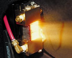 Laser diodes can be arrayed to produce very high power outputs, continuous wave or pulsed. Such arrays may be used to efficiently pump solid-state lasers for high average power drilling, burning or for inertial confinement fusion.
Laser diodes are numerically the most common laser type, with 2004 sales of approximately 733 million units,[6] as compared to 131,000 of other types of lasers.[7]
Laser diodes find wide use in telecommunication as easily modulated and easily coupled light sources for fiber optics communication. They are used in various measuring instruments, such as rangefinders. Another common use is in barcode readers. Visible lasers, typically red but later also green, are common as laser pointers. Both low and high-power diodes are used extensively in the printing industry both as light sources for scanning (input) of images and for very high-speed and high-resolution printing plate (output) manufacturing. Infrared and red laser diodes are common in CD players, CD-ROMs and DVD technology. Violet lasers are used in HD DVD and Blu-ray technology. Diode lasers have also found many applications in laser absorption spectrometry (LAS) for high-speed, low-cost assessment or monitoring of the concentration of various species in gas phase. High-power laser diodes are used in industrial applications such as heat treating, cladding, seam welding and for pumping other lasers, such as diode-pumped solid-state lasers.
Uses of laser diodes can be categorized in various ways. Most applications could be served by larger solid-state lasers or optical parametric oscillators, but the low cost of mass-produced diode lasers makes them essential for mass-market applications. Diode lasers can be used in a great many fields; since light has many different properties (power, wavelength, spectral and beam quality, polarization, etc.) it is useful to classify applications by these basic properties.
Many applications of diode lasers primarily make use of the "directed energy" property of an optical beam. In this category one might include the laser printers, barcode readers, image scanning, illuminators, designators, optical data recording, combustion ignition, laser surgery, industrial sorting, industrial machining, and directed energy weaponry. Some of these applications are well-established while others are emerging.
Laser medicine: medicine and especially dentistry have found many new uses for diode lasers.[8][9][10] The shrinking size of the units and their increasing user friendliness makes them very attractive to clinicians for minor soft tissue procedures. The 800 nm – 980 nm units have a high absorption rate for hemoglobin and thus make them ideal for soft tissue applications, where good hemostasis is necessary.
Uses which may make use of the coherence of diode-laser-generated light include interferometric distance measurement, holography, coherent communications, and coherent control of chemical reactions.
Uses which may make use of "narrow spectral" properties of diode lasers include range-finding, telecommunications, infra-red countermeasures, spectroscopic sensing, generation of radio-frequency or terahertz waves, atomic clock state preparation, quantum key cryptography, frequency doubling and conversion, water purification (in the UV), and photodynamic therapy (where a particular wavelength of light would cause a substance such as porphyrin to become chemically active as an anti-cancer agent only where the tissue is illuminated by light).
Uses where the desired quality of laser diodes is their ability to generate ultra-short pulses of light by the technique known as "mode-locking" include clock distribution for high-performance integrated circuits, high-peak-power sources for laser-induced breakdown spectroscopy sensing, arbitrary waveform generation for radio-frequency waves, photonic sampling for analog-to-digital conversion, and optical code-division-multiple-access systems for secure communication.
Common wavelengths
- 375 nm – excitation of Hoechst stain, Calcium Blue, and other fluorescent dyes in fluorescence microscopy
- 405 nm – InGaN blue-violet laser, in Blu-ray Disc and HD DVD drives
- 445 nm – InGaN Deep blue laser multimode diode recently introduced (2010) for use in mercury free high brightness data projectors
- 473 nm – Bright blue laser pointers, still very expensive, output of DPSS systems
- 485 nm – excitation of GFP and other fluorescent dyes
- 510 nm - Green diodes recently (2010) developed by Nichia for laser projectors.
- 635 nm – AlGaInP better red laser pointers, same power subjectively 5 times as bright as 670 nm one
- 640 nm – High brightness red DPSS laser pointers
- 657 nm – AlGaInP DVD drives, laser pointers
- 670 nm – AlGaInP cheap red laser pointers
- 760 nm – AlGaInP gas sensing: O2
- 785 nm – GaAlAs Compact Disc drives
- 808 nm – GaAlAs pumps in DPSS Nd:YAG lasers (e.g. in green laser pointers or as arrays in higher-powered lasers)
- 848 nm – laser mice
- 980 nm – InGaAs pump for optical amplifiers, for Yb:YAG DPSS lasers
- 1064 nm – AlGaAs fiber-optic communication, DPSS laser pump frequency
- 1310 nm – InGaAsP, InGaAsN fiber-optic communication
- 1480 nm – InGaAsP pump for optical amplifiers
- 1512 nm – InGaAsP gas sensing: NH3
- 1550 nm – InGaAsP, InGaAsNSb fiber-optic communication
- 1625 nm – InGaAsP fiber-optic communication, service channel
- 1654 nm – InGaAsP gas sensing: CH4
- 1877 nm – GaSbAs gas sensing: H2O
- 2004 nm – GaSbAs gas sensing: CO2
- 2330 nm – GaSbAs gas sensing: CO
- 2680 nm – GaSbAs gas sensing: CO2
History
Coherent light emission from a semiconductor (gallium arsenide) diode (the first laser diode) was demonstrated in 1962 by two US groups led by Robert N. Hall at the General Electric research center[11] and by Marshall Nathan at the IBM T.J. Watson Research Center.[12] The priority is given to General Electric group who have obtained and submitted their results earlier; they also went further and made a resonant cavity for their diode.[13] The first visible wavelength laser diode was demonstrated by Nick Holonyak, Jr. later in 1962.[14]
Other teams at MIT Lincoln Laboratory, Texas Instruments, and RCA Laboratories were also involved in and received credit for their historic initial demonstrations of efficient light emission and lasing in semiconductor diodes in 1962 and thereafter. GaAs lasers were also produced in early 1963 in the Soviet Union by the team led by Nikolay Basov.[15]
In the early 1960s liquid phase epitaxy (LPE) was invented by Herbert Nelson of RCA Laboratories. By layering the highest quality crystals of varying compositions, it enabled the demonstration of the highest quality heterojunction semiconductor laser materials for many years. LPE was adopted by all the leading laboratories, worldwide and used for many years. It was finally supplanted in the 1970s by molecular beam epitaxy and organometallic chemical vapor deposition.
Diode lasers of that era operated with threshold current densities of 1000 A/cm2 at 77 K temperatures. Such performance enabled continuous-lasing to be demonstrated in the earliest days. However, when operated at room temperature, about 300 K, threshold current densities were two orders of magnitude greater, or 100,000 A/cm2 in the best devices. The dominant challenge for the remainder of the 1960s was to obtain low threshold current density at 300 K and thereby to demonstrate continuous-wave lasing at room temperature from a diode laser.
The first diode lasers were homojunction diodes. That is, the material (and thus the bandgap) of the waveguide core layer and that of the surrounding clad layers, were identical. It was recognized that there was an opportunity, particularly afforded by the use of liquid phase epitaxy using aluminum gallium arsenide, to introduce heterojunctions. Heterostructures consist of layers of semiconductor crystal having varying bandgap and refractive index. Heterojunctions (formed from heterostructures) had been recognized by Herbert Kroemer, while working at RCA Laboratories in the mid-1950s, as having unique advantages for several types of electronic and optoelectronic devices including diode lasers. LPE afforded the technology of making heterojunction diode lasers.
The first heterojunction diode lasers were single-heterojunction lasers. These lasers utilized aluminum gallium arsenide p-type injectors situated over n-type gallium arsenide layers grown on the substrate by LPE. An admixture of aluminum replaced gallium in the semiconductor crystal and raised the bandgap of the p-type injector over that of the n-type layers beneath. It worked; the 300 K threshold currents went down by 10× to 10,000 amperes per square centimeter. Unfortunately, this was still not in the needed range and these single-heterostructure diode lasers did not function in continuous wave operation at room temperature.
The innovation that met the room temperature challenge was the double heterostructure laser. The trick was to quickly move the wafer in the LPE apparatus between different "melts" of aluminum gallium arsenide (p- and n-type) and a third melt of gallium arsenide. It had to be done rapidly since the gallium arsenide core region needed to be significantly under 1 µm in thickness. This may have been the earliest true example of "nanotechnology." The first laser diode to achieve continuous wave operation was a double heterostructure demonstrated in 1970 essentially simultaneously by Zhores Alferov and collaborators (including Dmitri Z. Garbuzov) of the Soviet Union, and Morton Panish and Izuo Hayashi working in the United States. However, it is widely accepted that Zhores I. Alferov and team reached the milestone first.[citation needed]
For their accomplishment and that of their co-workers, Alferov and Kroemer shared the 2000 Nobel Prize in Physics.
See also
- Laser diode rate equations
- Laser safety
- Collimating lens
- Superluminescent diode
- Millstone River Photonickers
References
- ^ M. Arrigoni, et. al., "Optically Pumped Semiconductor Lasers: Green OPSLs poised to enter scientific pump-laser market", OptoIQ (2009).
- ^ "Optically Pumped Semiconductor Laser (OPSL)", Sam's Laser FAQs.
- ^ Voumard, C. (1977). "External-cavity-controlled 32-MHz narrow-band cw GaA1As-diode lasers". Optics Letters 1 (2): 61–3. Bibcode 1977OptL....1...61V. doi:10.1364/OL.1.000061. PMID 19680331.
- ^ M. W. Fleming and A. Mooradian (1981). "Spectral characteristics of external-cavity controlled semiconductor lasers". IEEE J. Quantum Electron 17: 44–59. Bibcode 1981IJQE...17...44F. doi:10.1109/JQE.1981.1070634. http://ieeexplore.ieee.org/xpl/freeabs_all.jsp?arnumber=1070634.
- ^ P. Zorabedian (1995). "8". In F. J. Duarte. Tunable Lasers Handbook. Academic Press. ISBN 0-12-222695-X. http://books.google.com/?id=PPMC5BbSN0QC&printsec=frontcover.]
- ^ Steele, Robert V. (2005). "Diode-laser market grows at a slower rate". Laser Focus World 41 (2). http://lfw.pennnet.com/Articles/Article_Display.cfm?Section=ARCHI&ARTICLE_ID=221439&VERSION_NUM=4&p=12.
- ^ Kincade, Kathy; Stephen Anderson (2005). "Laser Marketplace 2005: Consumer applications boost laser sales 10%". Laser Focus World 41 (1). http://lfw.pennnet.com/Articles/Article_Display.cfm?section=ARCHI&ARTICLE_ID=219847&VERSION_NUM=2&p=12.
- ^ Yeh; Jain, K; Andreana, S (2005). "Using a diode laser to uncover dental implants in second-stage surgery". General dentistry 53 (6): 414–7. PMID 16366049.
- ^ Andreana (2005). "The use of diode lasers in periodontal therapy: literature review and suggested technique". Dentistry today 24 (11): 130, 132–5. PMID 16358809.
- ^ Deppe, Herbert; Horch, Hans-Henning (2007). "Laser applications in oral surgery and implant dentistry". Lasers in Medical Science 22 (4): 217–221. doi:10.1007/s10103-007-0440-3. PMID 17268764.
- ^ Hall, Robert N.; G. E. Fenner, J. D. Kingsley, T. J. Soltys, and R. O. Carlson (November 1962). "Coherent Light Emission From GaAs Junctions". Physical Review Letters 9 (9): 366–368. Bibcode 1962PhRvL...9..366H. doi:10.1103/PhysRevLett.9.366.
- ^ Nathan, Marshall I.; Dumke, William P.; Burns, Gerald; Dill, Frederick H.; Lasher, Gordon (1962). "Stimulated Emission of Radiation from GaAs p-n Junctions". Applied Physics Letters 1 (3): 62. Bibcode 1962ApPhL...1...62N. doi:10.1063/1.1777371. http://www.ecse.rpi.edu/~schubert/More-reprints/1962%20Nathan%20Dumke%20et%20al%20%28APL%29%20Stimulated%20emission%20of%20radiation%20from%20GaAs%20p-n%20junctions.pdf.
- ^ Oral History Transcript — Dr. Marshall Nathan, American Institute of Physics
- ^ "After Glow". Illinois Alumni Magazine. May–June 2007.
- ^ "Nicolay G. Basov". Nobelprize.org. http://nobelprize.org/nobel_prizes/physics/laureates/1964/basov-bio.html. Retrieved 2009-06-06.
Further reading
- B. Van Zeghbroeck's Principles of Semiconductor Devices( for direct and indirect band gaps)
- Saleh, Bahaa E. A. and Teich, Malvin Carl (1991). Fundamentals of Photonics. New York: John Wiley & Sons. ISBN 0-471-83965-5. ( For Stimulated Emission )
- Koyama et al., Fumio (1988), "Room temperature cw operation of GaAs vertical cavity surface emitting laser", Trans. IEICE, E71(11): 1089–1090( for VCSELS)
- Iga, Kenichi (2000), "Surface-emitting laser—Its birth and generation of new optoelectronics field", IEEE Journal of Selected Topics in Quantum Electronics 6(6): 1201–1215(for VECSELS)
- Duarte, F. J. (2009), "Broadly tunable dispersive external-cavity semiconductor lasers", in Tunable Laser Applications. New York: CRC Press. ISBN 1-4200-6009-0. pp. 143–177. (For external cavity diode lasers)
External links
- Sam's Laser FAQ by Samuel M. Goldwasser
- Britney Spears Guide to Semiconductor Physics Edge-emitting lasers
- Application and technical notes explaining current and temperature control of laser diodes
Categories:- Semiconductor lasers
- Optical diodes
- Heat-assisted magnetic recording
- Light sources


Wikimedia Foundation. 2010.