- Electron microscope
-
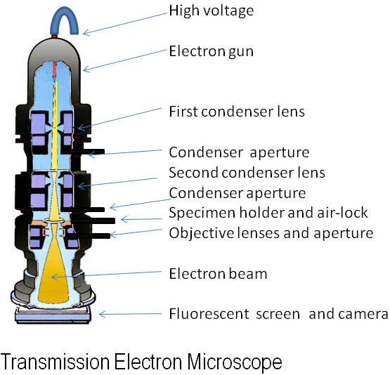
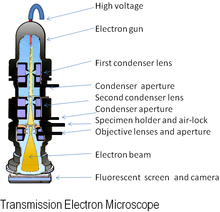 Diagram of a transmission electron microscope

An electron microscope is a type of microscope that uses a beam of electrons to illuminate the specimen and produce a magnified image. Electron microscopes (EM) have a greater resolving power than a light-powered optical microscope, because electrons have wavelengths about 100,000 times shorter than visible light (photons), and can achieve better than 50 pm resolution[1] and magnifications of up to about 10,000,000x, whereas ordinary, non-confocal light microscopes are limited by diffraction to about 200 nm resolution and useful magnifications below 2000x.
The electron microscope uses electrostatic and electromagnetic "lenses" to control the electron beam and focus it to form an image. These lenses are analogous to, but different from the glass lenses of an optical microscope that form a magnified image by focusing light on or through the specimen. In transmission, the electron beam is first diffracted by the specimen, and then, the electron microscope “lenses" re-focus the beam into a Fourier-transformed image of the diffraction pattern for the selected area of investigation. The real image thus formed is magnified by a factor ranging from a few hundred to many hundred thousand times, and can be viewed on a detecting screen or recorded using photographic film or plates or with a digital camera. Electron microscopes are used to observe a wide range of biological and inorganic specimens including microorganisms, cells, large molecules, biopsy samples, metals, and crystals. Industrially, the electron microscope is primarily used for quality control and failure analysis in semiconductor device fabrication.
Contents
History
 Electron microscope constructed by Ernst Ruska in 1933
The electron microscope was invented and patented by Hungarian physicist Leo Szilárd but declined to construct it.[2] Instead, German physicist Ernst Ruska and electrical engineer Max Knoll constructed the prototype electron microscope in 1931, capable of four-hundred-power magnification; the apparatus was a practical application of the principles of electron microscopy.[3] Two years later, in 1933, Ruska built an electron microscope that exceeded the resolution attainable with an optical (lens) microscope.[3] Moreover, Reinhold Rudenberg, the scientific director of Siemens-Schuckertwerke, obtained the patent for the electron microscope in May 1931. Family illness compelled the electrical engineer to devise an electrostatic microscope, because he wanted to make visible the poliomyelitis virus.
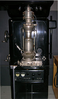
In 1932, Ernst Lubcke of Siemens & Halske built and obtained images from a prototype electron microscope, applying concepts described in the Rudenberg patent applications.[4] Five years later (1937), the firm financed the work of Ernst Ruska and Bodo von Borries, and employed Helmut Ruska (Ernst’s brother) to develop applications for the microscope, especially with biologic specimens.[3][5] Also in 1937, Manfred von Ardenne pioneered the scanning electron microscope.[6] The first practical electron microscope was constructed in 1938, at the University of Toronto, by Eli Franklin Burton and students Cecil Hall, James Hillier, and Albert Prebus; and Siemens produced the first commercial transmission electron microscope (TEM) in 1939.[7] Although contemporary electron microscopes are capable of two million-power magnification, as scientific instruments, they remain based upon Ruska’s prototype.
Types
Transmission electron microscope (TEM)
Main article: Transmission electron microscopeThe original form of electron microscope, the transmission electron microscope (TEM) uses a high voltage electron beam to create an image. The electrons are emitted by an electron gun, commonly fitted with a tungsten filament cathode as the electron source. The electron beam is accelerated by an anode typically at +100 keV (40 to 400 keV) with respect to the cathode, focused by electrostatic and electromagnetic lenses, and transmitted through the specimen that is in part transparent to electrons and in part scatters them out of the beam. When it emerges from the specimen, the electron beam carries information about the structure of the specimen that is magnified by the objective lens system of the microscope. The spatial variation in this information (the "image") is viewed by projecting the magnified electron image onto a fluorescent viewing screen coated with a phosphor or scintillator material such as zinc sulfide. The image can be photographically recorded by exposing a photographic film or plate directly to the electron beam, or a high-resolution phosphor may be coupled by means of a lens optical system or a fibre optic light-guide to the sensor of a CCD (charge-coupled device) camera. The image detected by the CCD may be displayed on a monitor or computer.
Resolution of the TEM is limited primarily by spherical aberration, but a new generation of aberration correctors have been able to partially overcome spherical aberration to increase resolution. Hardware correction of spherical aberration for the high-resolution transmission electron microscopy (HRTEM) has allowed the production of images with resolution below 0.5 angstrom (50 picometres)[1] and magnifications above 50 million times.[8] The ability to determine the positions of atoms within materials has made the HRTEM an important tool for nano-technologies research and development.[9]
The important mode of TEM utilization is electron diffraction. The advantages of electron diffraction over X-ray crystallography are that the specimen need not be a single crystal or even a polycrystalline powder, and also that the Fourier transform reconstruction of the object's magnified structure occurs physically and thus avoids the need for solving the phase problem faced by the X-ray crystallographers after obtaining their X-ray diffraction patterns of a single crystal or polycrystalline powder. The major disadvantage of the transmission electron microscope is the need for extremely thin sections of the specimens, typically about 100 nanometers. Biological specimens typically require to be chemically fixed, dehydrated and embedded in a polymer resin to stabilize them sufficiently to allow ultrathin sectioning. Sections of biological specimens, organic polymers and similar materials may require special `staining' with heavy atom labels in order to achieve the required image contrast.
Scanning electron microscope
Main article: Scanning electron microscope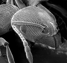 An image of an ant in a scanning electron microscope
Unlike the TEM, where electrons of the high voltage beam carry the image of the specimen, the electron beam of the scanning electron microscope (SEM)[10] does not at any time carry a complete image of the specimen. The SEM produces images by probing the specimen with a focused electron beam that is scanned across a rectangular area of the specimen (raster scanning). A point of the specimen, when in contact with the electron beam, generates several responses (signals), such as heat, emission of low-energy secondary electrons and high-energy backscattered electrons, light emission (cathodoluminescence) or X-ray emission. The display of the SEM maps the varying intensity of any of these signals into the image in a position corresponding to the position of the beam on the specimen when the signal was generated. In the SEM image of an ant shown at right, the image was constructed from signals produced by a secondary electron detector, the normal or conventional imaging mode in most SEMs.
Generally, the image resolution of an SEM is about an order of magnitude poorer than that of a TEM. However, because the SEM image relies on surface processes rather than transmission, it is able to image bulk samples up to many centimetres in size and (depending on instrument design and settings) has a great depth of field, and so can produce images that are good representations of the three-dimensional shape of the sample. Another advantage of SEM is its variety called environmental scanning electron microscope (ESEM) can produce images of sufficient quality and resolution with the samples being wet or contained in low vacuum or gas. This greatly facilitates imaging biological samples that are unstable in the high vacuum of conventional electron microscopes.
Reflection electron microscope
In the reflection electron microscope (REM) as in the TEM, an electron beam is incident on a surface, but instead of using the transmission (TEM) or secondary electrons (SEM), the reflected beam of elastically scattered electrons is detected. This technique is typically coupled with reflection high energy electron diffraction (RHEED) and reflection high-energy loss spectroscopy (RHELS). Another variation is spin-polarized low-energy electron microscopy (SPLEEM), which is used for looking at the microstructure of magnetic domains.[11]
Scanning transmission electron microscope
Main article: Scanning transmission electron microscopyThe STEM rasters a focused incident probe across a specimen that (as with the TEM) has been thinned to facilitate detection of electrons scattered through the specimen. The high resolution of the TEM is thus possible in STEM. The focusing action (and aberrations) occur before the electrons hit the specimen in the STEM, but afterward in the TEM. The STEMs use of SEM-like beam rastering simplifies annular dark-field imaging, and other analytical techniques, but also means that image data is acquired in serial rather than in parallel fashion.
Low-voltage electron microscope
The low-voltage electron microscope (LVEM) is a combination of SEM, TEM and STEM in one instrument, which operates at relatively low electron accelerating voltage of 5 kV. Low voltage reduces the specimen damage by the incident electrons and increases image contrast that is especially important for biological specimens. This increase in contrast significantly reduces, or even eliminates the need to stain. Sectioned samples generally need to be thinner than they would be for conventional TEM (20–65 nm). Resolutions of a few nm are possible in TEM, SEM and STEM modes.[12][13]
Sample preparation
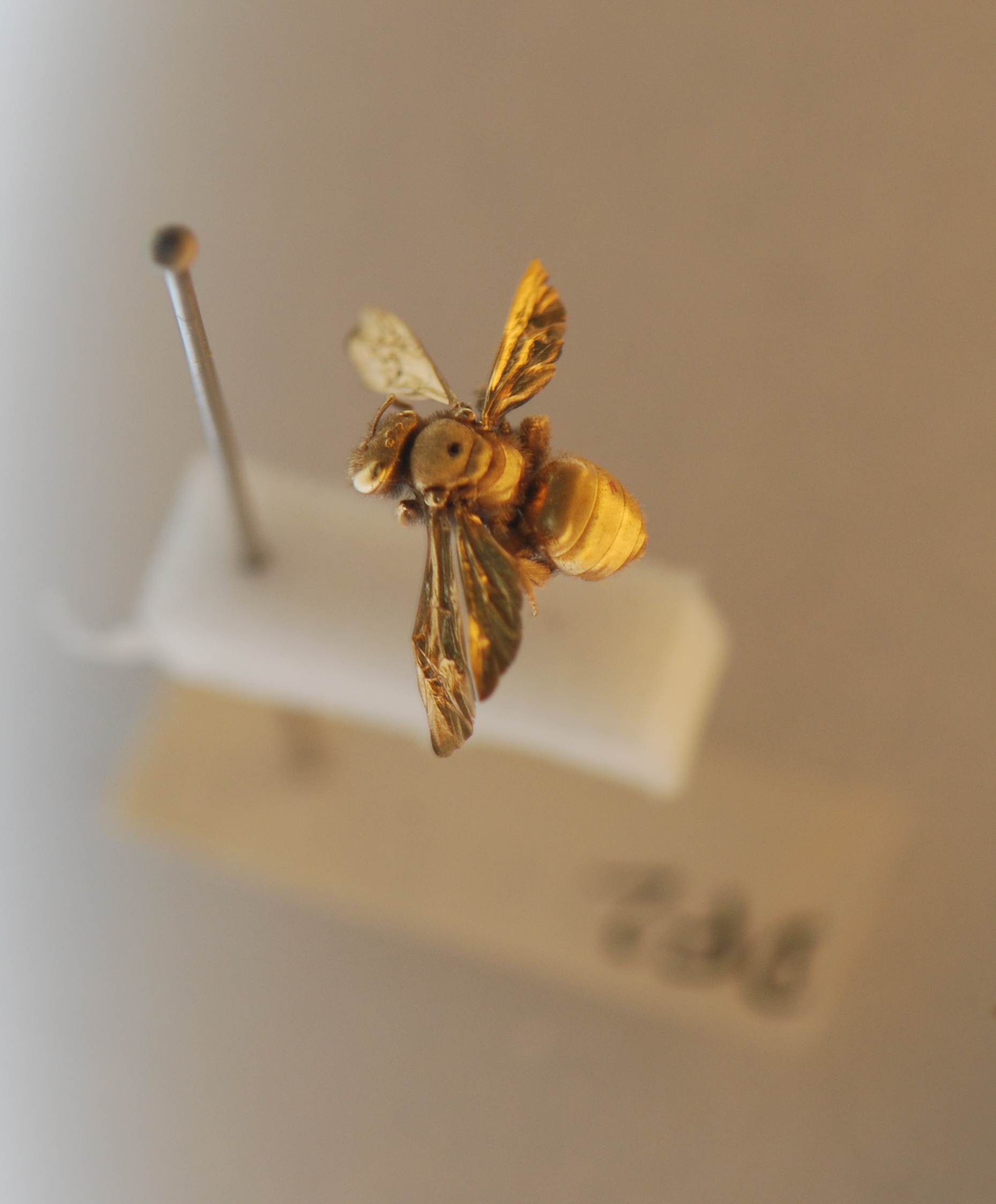
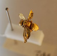 An insect coated in gold for viewing with a scanning electron microscope
Materials to be viewed under an electron microscope may require processing to produce a suitable sample. The technique required varies depending on the specimen and the analysis required:
- Chemical fixation – for biological specimens aims to stabilize the specimen's mobile macromolecular structure by chemical crosslinking of proteins with aldehydes such as formaldehyde and glutaraldehyde, and lipids with osmium tetroxide.
- Negative stain – suspensions containing fine biological material (such as viruses and bacteria) are briefly mixed with a dilute solution of an electron-opaque solution such as ammonium molybdate, uranyl acetate (or formate), or phosphotungstic acid. This mixture is applied to a suitably coated EM grid, blotted, then allowed to dry. Viewing of this preparation in the TEM should be carried out without delay for best results. The method is important in microbiology for fast but crude morphological identification, but can also be used as the basis for high resolution 3D reconstruction using EM tomography methodology when carbon films are used for support.
- Cryofixation – freezing a specimen so rapidly, to liquid nitrogen or even liquid helium temperatures, that the water forms vitreous (non-crystalline) ice. This preserves the specimen in a snapshot of its solution state. An entire field called cryo-electron microscopy has branched from this technique. With the development of cryo-electron microscopy of vitreous sections (CEMOVIS), it is now possible to observe samples from virtually any biological specimen close to its native state.[citation needed]
- Dehydration – freeze drying, or replacement of water with organic solvents such as ethanol or acetone, followed by critical point drying or infiltration with embedding resins.
- Embedding, biological specimens – after dehydration, tissue for observation in the transmission electron microscope is embedded so it can be sectioned ready for viewing. To do this the tissue is passed through a 'transition solvent' such as epoxy propane and then infiltrated with a resin such as Araldite epoxy resin; tissues may also be embedded directly in water-miscible acrylic resin. After the resin has been polymerised (hardened) the sample is thin sectioned (ultrathin sections) and stained – it is then ready for viewing.
- Embedding, materials – after embedding in resin, the specimen is usually ground and polished to a mirror-like finish using ultra-fine abrasives. The polishing process must be performed carefully to minimize scratches and other polishing artifacts that reduce image quality.
- Sectioning – produces thin slices of specimen, semitransparent to electrons. These can be cut on an ultramicrotome with a diamond knife to produce ultra-thin slices about 60–90 nm thick. Disposable glass knives are also used because they can be made in the lab and are much cheaper.
- Staining – uses heavy metals such as lead, uranium or tungsten to scatter imaging electrons and thus give contrast between different structures, since many (especially biological) materials are nearly "transparent" to electrons (weak phase objects). In biology, specimens can be stained "en bloc" before embedding and also later after sectioning. Typically thin sections are stained for several minutes with an aqueous or alcoholic solution of uranyl acetate followed by aqueous lead citrate.
- Freeze-fracture or freeze-etch – a preparation method particularly useful for examining lipid membranes and their incorporated proteins in "face on" view. The fresh tissue or cell suspension is frozen rapidly (cryofixation), then fractured by simply breaking or by using a microtome while maintained at liquid nitrogen temperature. The cold fractured surface (sometimes "etched" by increasing the temperature to about −100 °C for several minutes to let some ice sublime) is then shadowed with evaporated platinum or gold at an average angle of 45° in a high vacuum evaporator. A second coat of carbon, evaporated perpendicular to the average surface plane is often performed to improve stability of the replica coating. The specimen is returned to room temperature and pressure, then the extremely fragile "pre-shadowed" metal replica of the fracture surface is released from the underlying biological material by careful chemical digestion with acids, hypochlorite solution or SDS detergent. The still-floating replica is thoroughly washed free from residual chemicals, carefully fished up on fine grids, dried then viewed in the TEM.
- Ion beam milling – thins samples until they are transparent to electrons by firing ions (typically argon) at the surface from an angle and sputtering material from the surface. A subclass of this is focused ion beam milling, where gallium ions are used to produce an electron transparent membrane in a specific region of the sample, for example through a device within a microprocessor. Ion beam milling may also be used for cross-section polishing prior to SEM analysis of materials that are difficult to prepare using mechanical polishing.
- Conductive coating – an ultrathin coating of electrically conducting material, deposited either by high vacuum evaporation or by low vacuum sputter coating of the sample. This is done to prevent the accumulation of static electric fields at the specimen due to the electron irradiation required during imaging. The coating materials include gold, gold/palladium, platinum, tungsten, graphite, etc. Coating is especially important for the study of specimens with the scanning electron microscope where electrons are accelerated by a relatively low voltage and therefore are affected more by the sample charging. Another reason for coating, even when there is more than enough conductivity, is to improve contrast, a situation more common with the operation of an FESEM (field emission SEM).
Disadvantages
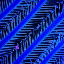 False-color SEM image of the filter setae of an Antarctic krill. (Raw electron microscope images carry no color information.)
Pictured: First degree filter setae with a V pattern of second degree setae pointing towards the inside of the feeding basket. The purple ball is 1 µm in diameter.Electron microscopes are expensive to build and maintain, but the capital and running costs of confocal light microscope systems now overlaps with those of basic electron microscopes. They are dynamic rather than static in their operation, requiring extremely stable high-voltage supplies, extremely stable currents to each electromagnetic coil/lens, continuously pumped high- or ultra-high-vacuum systems, and a cooling water supply circulation through the lenses and pumps. As they are very sensitive to vibration and external magnetic fields, microscopes designed to achieve high resolutions must be housed in stable buildings (sometimes underground) with special services such as magnetic field cancelling systems. Some desktop low-voltage electron microscopes have TEM capabilities at relatively low voltages (around 5 kV) without stringent voltage supply, lens coil current, cooling water or vibration isolation requirements and as such are much less expensive to buy and far easier to install and maintain, but do not have the same ultra-high (atomic scale) resolution capabilities as the larger instruments.
The samples largely have to be viewed in vacuum, as the molecules that make up air would scatter the electrons. One exception is the environmental scanning electron microscope, which allows hydrated samples to be viewed in a low-pressure (up to 20 Torr/2.7 kPa), wet environment.
Scanning electron microscopes operating in conventional high-vacuum mode usually image conductive specimens; therefore non-conductive materials require conductive coating (gold/palladium alloy, carbon, osmium, etc.) Low-voltage mode of modern microscopes makes possible observation of non-conductive specimens without coating. Non-conductive materials can be imaged also by an variable pressure (or environmental) scanning electron microscope.
Small, stable specimens such as carbon nanotubes, diatom frustules and small mineral crystals (asbestos fibres, for example) require no special treatment before being examined in the electron microscope. Samples of hydrated materials, including almost all biological specimens have to be prepared in various ways to stabilize them, reduce their thickness (ultrathin sectioning) and increase their electron optical contrast (staining). These processes may result in artifacts, but these can usually be identified by comparing the results obtained by using radically different specimen preparation methods. It is generally believed by scientists working in the field that as results from various preparation techniques have been compared and that there is no reason that they should all produce similar artifacts, it is reasonable to believe that electron microscopy features correspond with those of living cells. Since the 1980s, analysis of cryofixed, vitrified specimens has also become increasingly used by scientists, further confirming the validity of this technique.[14][15][16]
Applications
- Semiconductor and data storage
- Circuit edit
- Defect analysis
- Failure analysis
Biology and life sciences
- Diagnostic electron microscopy
- Cryobiology
- Protein localization
- Electron tomography
- Cellular tomography
- Cryo-electron microscopy
- Toxicology
- Biological production and viral load monitoring
- Particle analysis
- Pharmaceutical QC
- Structural biology
- 3D tissue imaging
- Virology
- Vitrification
- Research
- Electron beam-induced deposition
- Materials qualification
- Materials and sample preparation
- Nanoprototyping
- Nanometrology
- Device testing and characterization
- Industry
- High-resolution imaging
- 2D & 3D micro-characterization
- Macro sample to nanometer metrology
- Particle detection and characterization
- Direct beam-writing fabrication
- Dynamic materials experiments
- Sample preparation
- Forensics
- Mining (mineral liberation analysis)
- Chemical/Petrochemical
See also
- Category:Electron microscope images
- Electron energy loss spectroscopy (EELS)
- Energy filtered transmission electron microscopy (EFTEM)
- Field emission microscope
- HiRISE
- Scanning tunneling microscope
- Scanning confocal electron microscopy
- Scanning electron microscope (SEM)
- Transmission Electron Aberration-corrected Microscope
- Electron diffraction
- X-ray diffraction
- X-ray microscope
- X-ray photoelectron spectroscopy (XPS)
- Microscope image processing
- Microscopy
- Acronyms in microscopy
- Nanoscience
- Nanotechnology
- Surface science
- Ultramicroscopy (journal)
References
- ^ a b Erni, Rolf; Rossell, MD; Kisielowski, C; Dahmen, U (2009). "Atomic-Resolution Imaging with a Sub-50-pm Electron Probe". Physical Review Letters 102 (9): 096101. Bibcode 2009PhRvL.102i6101E. doi:10.1103/PhysRevLett.102.096101. PMID 19392535.
- ^ Gene Dannen: Leo Szilard the Inventor: A Slideshow (1998, Budapest, conference talk) http://www.dannen.com/budatalk.html
- ^ a b c Ernst Ruska (1986). "Ernst Ruska Autobiography". Nobel Foundation. http://nobelprize.org/nobel_prizes/physics/laureates/1986/ruska-autobio.html. Retrieved 2010-01-31.
- ^ H Gunther Rudenberg and Paul G Rudenberg (2010). "Origin and Background of the Invention of the Electron Microscope: Commentary". Advances in Imaging and Electron Physics (Elsevier) 160.
- ^ Kruger DH, Schneck P, Gelderblom HR (May 2000). "Helmut Ruska and the visualisation of viruses". Lancet 355 (9216): 1713–7. doi:10.1016/S0140-6736(00)02250-9. PMID 10905259. http://linkinghub.elsevier.com/retrieve/pii/S0140673600022509.
- ^ M von Ardenne and D Beischer (1940). "Untersuchung von metalloxyd-rauchen mit dem universal-elektronenmikroskop" (in German). Zeitschrift Electrochemie 46: 270–277. doi:10.1002/bbpc.19400460406.
- ^ "James Hillier". Inventor of the Week: Archive. 2003-05-01. http://web.mit.edu/Invent/iow/hillier.html. Retrieved 2010-01-31.
- ^ "The Scale of Things". Office of Basic Energy Sciences, U.S. Department of Energy. 2006-05-26. http://www.sc.doe.gov/bes/scale_of_things.html. Retrieved 2010-01-31.
- ^ O'Keefe MA, Allard LF (pdf). Sub-Ångstrom Electron Microscopy for Sub-Ångstrom Nano-Metrology. Information Bridge: DOE Scientific and Technical Information – Sponsored by OSTI. http://www.osti.gov/bridge/servlets/purl/821768-E3YVgN/native/821768.pdf. Retrieved 2010-01-31.
- ^ McMullan D (1993). "Scanning Electron Microscopy, 1928–1965". 51st Annual Meeting of the Microscopy Society of America. Cincinnati, OH. http://www-g.eng.cam.ac.uk/125/achievements/mcmullan/mcm.htm. Retrieved 2010-01-31.
- ^ "SPLEEM". National Center for Electron Microscopy (NCEM). http://ncem.lbl.gov/frames/spleem.html. Retrieved 2010-01-31.
- ^ Nebesářová1, Jana; Vancová, Marie (2007). "How to Observe Small Biological Objects in Low-Voltage Electron Microscope". Microscopy and Microanalysis 13 (3): 248–249. doi:10.1017/S143192760708124X. http://journals.cambridge.org/abstract_S143192760708124X.
- ^ Drummy, Lawrence, F.; Yang, Junyan; Martin, David C. (2004). "Low-voltage electron microscopy of polymer and organic molecular thin films". Ultramicroscopy 99 (4): 247–256. doi:10.1016/j.ultramic.2004.01.011. PMID 15149719.
- ^ Adrian, Marc; Dubochet, Jacques; Lepault, Jean; McDowall, Alasdair W. (1984). "Cryo-electron microscopy of viruses". Nature 308 (5954): 32–36. Bibcode 1984Natur.308...32A. doi:10.1038/308032a0. PMID 6322001.
- ^ Sabanay, I.; Arad, T.; Weiner, S.; Geiger, B. (1991). "Study of vitrified, unstained frozen tissue sections by cryoimmunoelectron microscopy". Journal of Cell Science 100 (1): 227–236. PMID 1795028.
- ^ Kasas, S.; Dumas, G.; Dietler, G.; Catsicas, S.; Adrian, M. (2003). "Vitrification of cryoelectron microscopy specimens revealed by high-speed photographic imaging". Journal of Microscopy 211 (1): 48–53. doi:10.1046/j.1365-2818.2003.01193.x.
External links
- Science Aid: Electron Microscopy High School (GCSE, A Level) resource
- Cell Centered Database – Electron microscopy data
General
- Nanohedron.com|Nano image gallery beautiful images generated with electron microscopes.
- electron microscopy Website of the ETH Zurich: Very good graphics and images, which illustrate various procedures.
- Environmental Scanning Electron Microscope (ESEM)
- X-ray element analysis in electron microscope – Information portal with X-ray microanalysis and EDX contents
- Introduction to Electron Microscopy by Eva Nogales (UC Berkeley)
History
- John H.L. Watson: Very early Electron Microscopy in the Department of Physics, the University of Toronto – A personal recollection
- Rubin Borasky Electron Microscopy Collection, 1930–1988 Archives Center, National Museum of American History, Smithsonian Institution.
Other
Categories:- Electron microscopy
- Scientific techniques


Wikimedia Foundation. 2010.