- Integrated circuit design
-
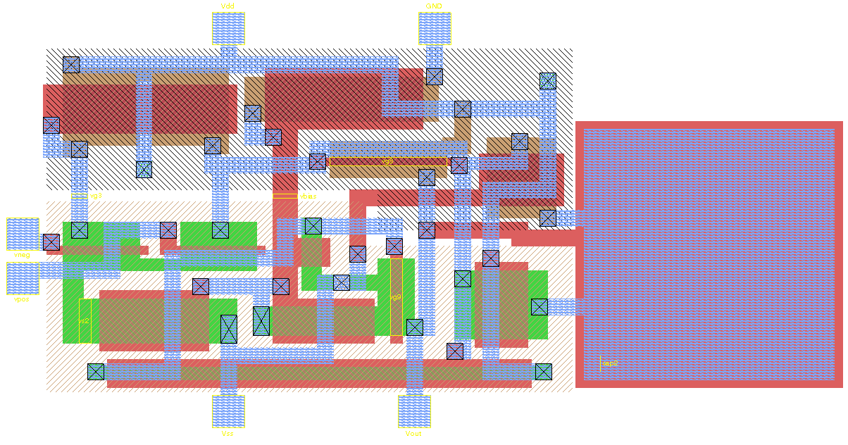
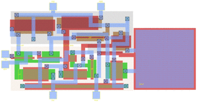 Layout view of a simple CMOS Operational Amplifier ( inputs are to the left and the compensation capacitor is to the right ). The metal layers are colored blue and green, the polysilicon is red and vias are crosses.
Integrated circuit design, or IC design, is a subset of electrical engineering and computer engineering, encompassing the particular logic and circuit design techniques required to design integrated circuits, or ICs. ICs consist of miniaturized electronic components built into an electrical network on a monolithic semiconductor substrate by photolithography.
IC design can be divided into the broad categories of digital and analog IC design. Digital IC design is to produce components such as microprocessors, FPGAs, memories (RAM, ROM, and flash) and digital ASICs. Digital design focuses on logical correctness, maximizing circuit density, and placing circuits so that clock and timing signals are routed efficiently. Analog IC design also has specializations in power IC design and RF IC design. Analog IC design is used in the design of op-amps, linear regulators, phase locked loops, oscillators and active filters. Analog design is more concerned with the physics of the semiconductor devices such as gain, matching, power dissipation, and resistance. Fidelity of analog signal amplification and filtering is usually critical and as a result, analog ICs use larger area active devices than digital designs and are usually less dense in circuitry.
Modern ICs are enormously complicated. A large chip, as of 2009 has close to 1 billion transistors. The rules for what can and cannot be manufactured are also extremely complex. An IC process as of 2006 may well have more than 600 rules. Furthermore, since the manufacturing process itself is not completely predictable, designers must account for its statistical nature. The complexity of modern IC design, as well as market pressure to produce designs rapidly, has led to the extensive use of automated design tools in the IC design process. In short, the design of an IC using EDA software is the design, test, and verification of the instructions that the IC is to carry out.
Contents
Fundamentals
Integrated circuit design involves the creation of electronic components, such as transistors, resistors, capacitors and the metallic interconnect of these components onto a piece of semiconductor, typically silicon. A method to isolate the individual components formed in the substrate is necessary since the substrate silicon is conductive and often forms an active region of the individual components. The two common methods are p-n junction isolation and dielectric isolation. Attention must be given to power dissipation of transistors and interconnect resistances and current density of the interconnect, contacts and vias since ICs contain very tiny devices compared to discrete components, where such concerns are less of an issue. Electromigration in metallic interconnect and ESD damage to the tiny components are also of concern. Finally, the physical layout of certain circuit subblocks is typically critical, in order to achieve the desired speed of operation, to segregate noisy portions of an IC from quiet portions, to balance the effects of heat generation across the IC, or to facilitate the placement of connections to circuitry outside the IC.
Design steps
A typical IC design cycle involves several steps:
- Feasibility study and die size estimate
- Functional verification
- Circuit/RTL design
- Circuit/RTL simulation Logic simulation
- Floorplanning
- Design review
- Layout
- Layout verification
- Static timing analysis
- Layout review
- Design For Test and Automatic test pattern generation
- Design for manufacturability (IC)
- Mask data preparation
- Wafer fabrication
- Die test
- Packaging
- Post silicon validation&integration
- Device characterization
- Tweak (if necessary)
- Datasheet generation Portable Document Format
- Ramp up
- Production
- Yield Analysis / Warranty Analysis Reliability (semiconductor)
- Failure analysis on any returns
- Plan for next generation chip using production information if possible
Digital design
Roughly speaking, digital IC design can be divided into three parts.
- Electronic system-level design: This step creates the user functional specification. The user may use a variety of languages and tools to create this description. Examples include a C/C++ model, SystemC, SystemVerilog Transaction Level Models, Simulink and MATLAB.
- RTL design: This step converts the user specification (what the user wants the chip to do) into a register transfer level (RTL) description. The RTL describes the exact behavior of the digital circuits on the chip, as well as the interconnections to inputs and outputs.
- Physical design: This step takes the RTL, and a library of available logic gates, and creates a chip design. This involves figuring out which gates to use, defining places for them, and wiring them together.
Note that the second step, RTL design, is responsible for the chip doing the right thing. The third step, physical design, does not affect the functionality at all (if done correctly) but determines how fast the chip operates and how much it costs.
RTL design
This is the hardest part, and the domain of functional verification. The spec may have some terse description, such as encodes in the MP3 format or implements IEEE floating-point arithmetic. Each of these innocent looking statements expands to hundreds of pages of text, and thousands of lines of computer code. It is extremely difficult to verify that the RTL will do the right thing in all the possible cases that the user may throw at it. Many techniques are used, none of them perfect but all of them useful – extensive logic simulation, formal methods, hardware emulation, lint-like code checking, and so on.
A tiny error here can make the whole chip useless, or worse. The famous Pentium FDIV bug caused the results of a division to be wrong by at most 61 parts per million, in cases that occurred very infrequently. No one even noticed it until the chip had been in production for months. Yet Intel was forced to offer to replace, for free, every chip sold until they could fix the bug, at a cost of $475 million (US).
Physical design
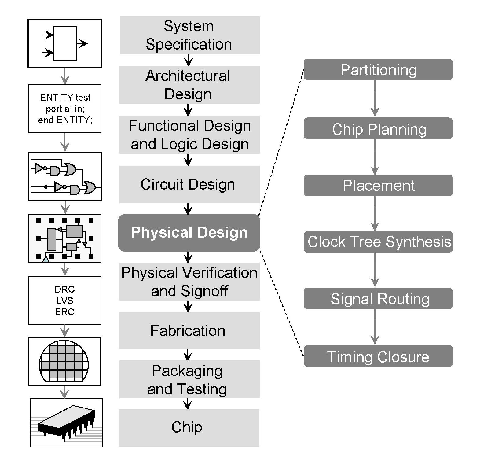
 VLSI circuit design flow with a focus on physical design
Here are the main steps of physical design. In practice there is not a straightforward progression - considerable iteration is required to ensure all objectives are met simultaneously. This is a difficult problem in its own right, called design closure.
- Floorplanning: The RTL of the chip is assigned to gross regions of the chip, input/output (I/O) pins are assigned and large objects (arrays, cores, etc.) are placed.
- Logic synthesis: The RTL is mapped into a gate-level netlist in the target technology of the chip.
- Placement: The gates in the netlist are assigned to nonoverlapping locations on the die area.
- Logic/placement refinement: Iterative logical and placement transformations to close performance and power constraints.
- Clock insertion: Clock signal wiring is (commonly, clock trees) introduced into the design.
- Routing: The wires that connect the gates in the netlist are added.
- Postwiring optimization: Performance (timing closure), noise (signal integrity), and yield (Design for manufacturability) violations are removed.
- Design for manufacturability: The design is modified, where possible, to make it as easy and efficient as possible to produce. This is achieved by adding extra vias or adding dummy metal/diffusion/poly layers wherever possible while complying to the design rules set by the foundry.
- Final checking: Since errors are expensive, time consuming and hard to spot, extensive error checking is the rule, making sure the mapping to logic was done correctly, and checking that the manufacturing rules were followed faithfully.
- Tapeout and mask generation: the design data is turned into photomasks in mask data preparation.
Process corners
Process corners provide digital designers the ability to simulate the circuit while accounting for variations in the technology process.
Analog design
Before the advent of the microprocessor and software based design tools, analog ICs were designed using hand calculations. These ICs were basic circuits, op-amps are one example, usually involving no more than ten transistors and few connections. An iterative trial-and-error process and "overengineering" of device size was often necessary to achieve a manufacturable IC. Reuse of proven designs allowed progressively more complicated ICs to be built upon prior knowledge. When inexpensive computer processing became available in the 1970s, computer programs were written to simulate circuit designs with greater accuracy than practical by hand calculation. The first circuit simulator for analog ICs was called SPICE (Simulation Program with Integrated Circuits Emphasis). Computerized circuit simulation tools enable greater IC design complexity than hand calculations can achieve, making the design of analog ASICs practical. The computerized circuit simulators also enable mistakes to be found early in the design cycle before a physical device is fabricated. Additionally, a computerized circuit simulator can implement more sophisticated device models and circuit analysis too tedious for hand calculations, permitting Monte Carlo analysis and process sensitivity analysis to be practical. The effects of parameters such as temperature variation, doping concentration variation and statistical process variations can be simulated easily to determine if an IC design is manufacturable. Overall, computerized circuit simulation enables a higher degree of confidence that the circuit will work as expected upon manufacture.
Coping with variability
A challenge most critical to analog IC design involves the variability of the individual devices built on the semiconductor chip. Unlike board-level circuit design which permits the designer to select devices that have each been tested and binned according to value, the device values on an IC can vary widely which are uncontrollable by the designer. For example, some IC resistors can vary ±20% and β of an integrated BJT can vary from 20 to 100. To add to the design challenge, device properties often vary between each processed semiconductor wafer. Device properties can even vary significantly across each individual IC due to doping gradients. The underlying cause of this variability is that many semiconductor devices are highly sensitive to uncontrollable random variances in the process. Slight changes to the amount of diffusion time, uneven doping levels, etc. can have large effects on device properties.
Some design techniques used to reduce the effects of the device variation are:
- Using the ratios of resistors, which do match closely, rather than absolute resistor value.
- Using devices with matched geometrical shapes so they have matched variations.
- Making devices large so that statistical variations becomes an insignificant fraction of the overall device property.
- Segmenting large devices, such as resistors, into parts and interweaving them to cancel variations.
- Using common centroid device layout to cancel variations in devices which must match closely (such as the transistor differential pair of an op amp).
Vendors
The four largest companies[citation needed] selling electronic design automation tools are Synopsys, Cadence, Mentor Graphics, and Magma.
See also
- Electronic circuit design
- Electronic design automation
- Power network design (IC)
- IEEE Transactions on Computer-Aided Design of Integrated Circuits and Systems
References
- Electronic Design Automation For Integrated Circuits Handbook, by Lavagno, Martin, and Scheffer, ISBN 0-8493-3096-3 A survey of the field of electronic design automation, one of the main enablers of modern IC design.
External links
Categories:- Integrated circuits
- Electronic design
- Electronic engineering
Wikimedia Foundation. 2010.