- Photomask
-
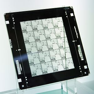 A photomask.
 A schematic illustration of a photomask (top) and an integrated circuit created using that mask (bottom).
A photomask is an opaque plate with holes or transparencies that allow light to shine through in a defined pattern. They are commonly used in photolithography.
Contents
Overview
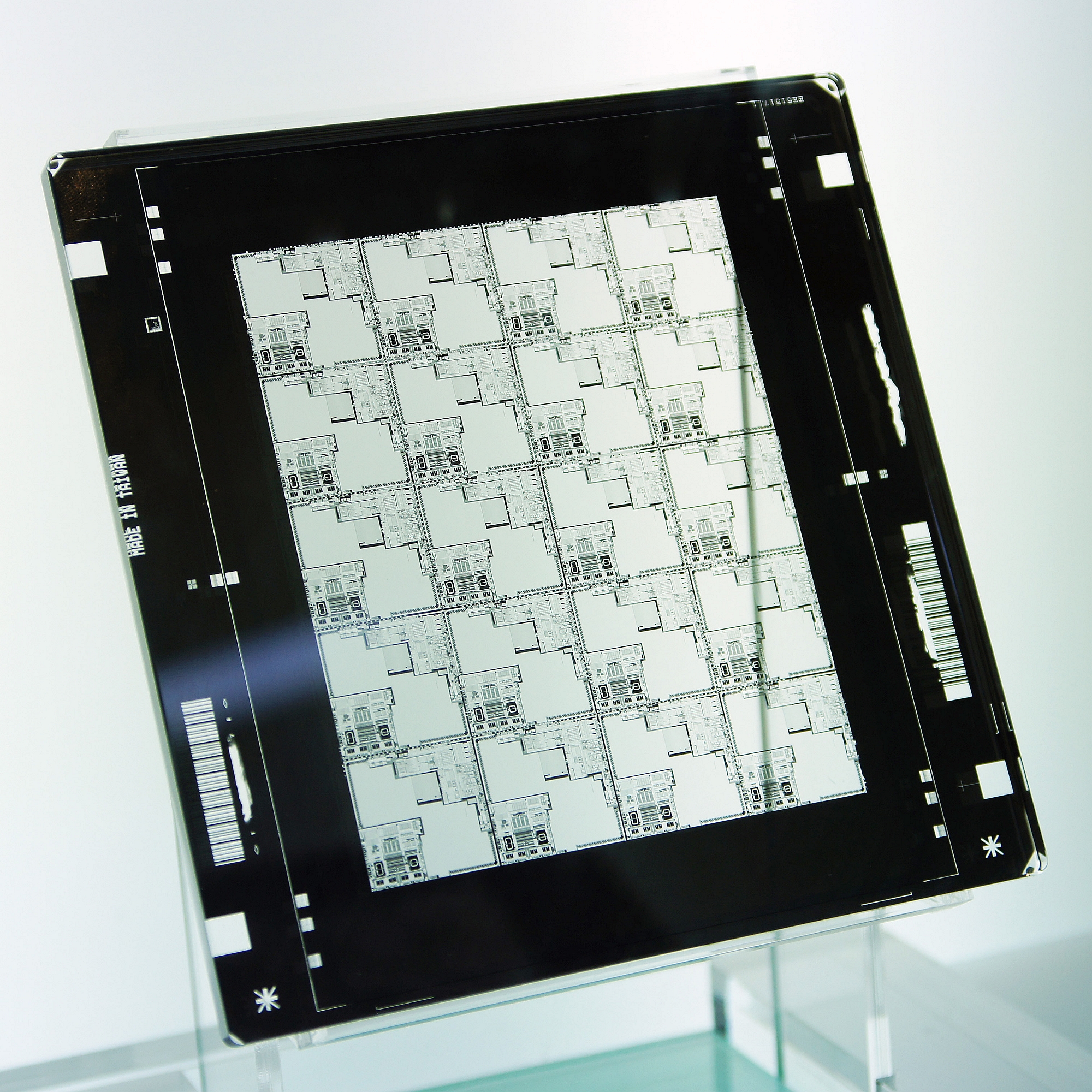
 An actual photomask. The thicker features are the integrated circuit which is desired to be printed on the wafer. The thinner features are assists which do not print themselves but help the integrated circuit print better out-of-focus. The zig-zag appearance of the photomask is because optical proximity correction was applied to it to make it print better.
Lithographic photomasks are typically transparent fused silica blanks covered with a pattern defined with a chrome metal absorbing film. Photomasks are used at wavelengths of 365 nm, 248 nm, and 193 nm. Photomasks have also been developed for other forms of radiation such as 157 nm, 13.5 nm (EUV), X-ray and electrons and ions, but these require entirely new materials for the substrate and the pattern film.
A set of photomasks, each defining a pattern layer in integrated circuit fabrication, is fed into a photolithography stepper or scanner and individually selected for exposure. In double patterning techniques, a photomask would correspond to a subset of the layer pattern.
In photolithography for the mass production of integrated circuit devices, the more correct term is usually photoreticle or simply reticle. In the case of a photomask, there is a one-to-one correspondence between the mask pattern and the wafer pattern. This was the standard for the 1:1 mask aligners that were succeeded by steppers and scanners with reduction optics. As used in steppers and scanners, the reticle commonly contains only one layer of the chip. (However, some photolithography fabs utilize reticles with more than one layer patterned onto the same mask). The pattern is projected and shrunk by four or five times onto the wafer surface. To achieve complete wafer coverage, the wafer is repeatedly 'stepped' from position to position under the optical column until full exposure is achieved.
Features 150 nm or below in size generally require phase-shifting to enhance the image quality to acceptable values. This can be achieved in many ways, but the two most common methods are to use an attenuated phase-shifting background film on the mask to increase the contrast of small intensity peaks, or to etch the exposed quartz so that the edge between the etched and unetched areas can be used to image nearly zero intensity. In the second case, unwanted edges would need to be trimmed out with another exposure. The former method is attenuated phase-shifting, and is often considered a weak enhancement, requiring special illumination for the most enhancement, while the latter method is known as alternating-aperture phase-shifting, and is the most popular strong enhancement technique.
As leading-edge semiconductor features shrink, photomask features which are 4× larger must inevitably shrink as well. This could pose challenges as the absorber film will need to become thinner, and hence less opaque.[1] A recent study by IMEC has found that thinner absorbers degrade image contrast and hence contribute to line-edge roughness, using state-of-the-art photolithography tools.[2] One possibility is to eliminate absorbers altogether and use 'chromeless' masks, relying solely on phase-shifting for imaging.
The emergence of immersion lithography has a strong impact on photomask requirements. The commonly used attenuated phase-shifting mask is more sensitive to the higher incidence angles applied in "hyper-NA" lithography, due to the longer optical path through the patterned film.[3]
Mask Error Enhancement Factor
Leading edge photomasks contain (pre-corrected) images of the final chip patterns magnified by 4x. This magnification factor has been a key benefit in reducing pattern sensitivity to imaging errors. However, as features continue to shrink, two trends come into play: 1) the mask error factor begins to exceed 1, i.e., the dimension error on the wafer may be more than 1/4 the dimension error on the mask,[4] and 2) the mask feature is becoming smaller, and the dimension tolerance is approaching a few nanometers. As an example, a 25 nm wafer pattern should correspond to a 100 nm mask pattern, but the wafer tolerance could be 1.25 nm (5% spec) which translates into 5 nm on the photomask. The variation of electron beam scattering in directly writing the photomask pattern can easily well exceed this.[5][6]
Pellicles
Particle contamination can be a significant problem in semiconductor manufacturing. A photomask is protected from particles by a pellicle – a thin transparent film stretched over a frame that is glued over one side of the photomask. The pellicle is far enough away from the mask patterns so that moderate-to-small sized particles that land on the pellicle will be too far out of focus to print. Although they are designed to keep particles away, pellicles become a part of the imaging system and their optical properties need to be taken into account.[7]
Leading commercial photomask manufacturers
The SPIE Annual Conference, Photomask Technology reports the SEMATECH Mask Industry Assessment which includes current industry analysis and the results of their annual photomask manufacturers survey. The following companies are listed in order of their global market share (2009 info).[8]
- Dai Nippon Printing Company
- Toppan Photomasks
- Photronics Inc
- Hoya Japan
- Taiwan Mask Corporation
- Compugraphics Photomask Solutions
Major chipmakers such as Intel, AMD, IBM, NEC, TSMC, Samsung, Micron Technology, etc., have their own large maskmaking facilities.
- Photo Sciences, Inc. is the largest privately held photomask manufacturer in the United States, 2009.
The cost to set up a modern 45 nm process mask shop is US$200-500 million, a very high threshold for entering this market. The purchase price of a photomask can range from $1,000 to $100,000 for a single, high end phase shift mask; as many as 30 masks (of varying price) may be required to form a complete mask set.
See also
References
- ^ Y. Sato et al., Proc. SPIE, vol. 4889, pp. 50-58 (2002).
- ^ M. Yoshizawa et al., Proc. SPIE, vol. 5853, pp. 243-251 (2005)
- ^ C. A. Mack et al., Proc. SPIE, vol. 5992, pp. 306-316 (2005)
- ^ E. Hendrickx et al., Proc. SPIE 7140, 714007 (2008).
- ^ C-J. Chen et al., Proc. SPIE 5256, 673 (2003).
- ^ W-H. Cheng and J. Farnsworth, Proc. SPIE 6607, 660724 (2007).
- ^ Chris A. Mack (November 2007). "Optical behavior of pellicles". Microlithography World. http://www.solid-state.com/display_article/311163/28/none/none/Feat/The-Lithography-Expert-Optical-behavior-of-pellicles. Retrieved 2008-09-13.
- ^ G Hughes and H Yun, Proc. SPIE 7488, 748802 (2009)
External links
Categories:- Lithography (microfabrication)


Wikimedia Foundation. 2010.