- Electromigration
-
Electromigration is the transport of material caused by the gradual movement of the ions in a conductor due to the momentum transfer between conducting electrons and diffusing metal atoms. The effect is important in applications where high direct current densities are used, such as in microelectronics and related structures. As the structure size in electronics such as integrated circuits (ICs) decreases, the practical significance of this effect increases.
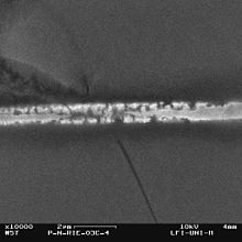 SEM image of a failure caused by electromigration in a copper interconnect. The passivation has been removed by RIE and HF
Contents
History
The phenomenon of electromigration has been known for over 100 years, having been discovered by the French scientist Gerardin.[1] The topic first became of practical interest in 1966 when the first integrated circuits became commercially available. Research in this field was pioneered by a number of investigators throughout the fledgling semiconductor industry. One of the most important engineering studies was performed by Jim Black of Motorola, after whom Black's equation is named. At the time, the metal interconnects in ICs were still about 10 micrometres wide. Currently interconnects are only hundreds to tens of nanometers in width, making research in electromigration increasingly important.
Practical implications of electromigration
Electromigration decreases the reliability of chips ( integrated circuits (ICs) ). It can cause the eventual loss of connections or failure of a circuit. Since reliability is important for space travel, military purposes, anti-lock braking system, medical equipment like Automated External Defibrillators and even computers or home entertainment systems, it is an important issue for economic and Human safety/survival reasons.
Due to difficulty of testing under real conditions, Black's equation is used to predict the life span of integrated circuits. To use Black's equation, the component is put through high temperature operating life (HTOL) testing. The component's expected life span under real conditions is extrapolated from data gathered during the testing.
Although electromigration damage ultimately results in failure of the affected IC, the first symptoms are intermittent glitches, and are quite challenging to diagnose. As some interconnects fail before others, the circuit exhibits seemingly random errors, which may be indistinguishable from other failure mechanisms (such as electrostatic discharge damage). In a laboratory setting, electromigration failure is readily imaged with an electron microscope, as interconnect erosion leaves telltale visual markers on the metal layers of the IC.
With increasing miniaturization the probability of failure due to electromigration increases in VLSI and ULSI circuits because both the power density and the current density increase. In advanced semiconductor manufacturing processes, copper has replaced aluminium as the interconnect material of choice. Despite its greater fragility in the fabrication process, copper is preferred for its superior conductivity. It is also intrinsically less susceptible to electromigration. However, electromigration (EM) continues to be an ever present challenge to device fabrication, and therefore the EM research for copper interconnects is ongoing (though a relatively new field).
A reduction of the structure (scaling) by a factor k increases the power density proportional to k and the current density increases by k2 whereby EM is clearly strengthened.
In modern consumer electronic devices, ICs rarely fail due to electromigration effects. This is because proper semiconductor design practices incorporate the effects of electromigration into the IC's layout. Nearly all IC design houses use automated EDA tools to check and correct electromigration problems at the transistor layout-level. When operated within the manufacturer's specified temperature and voltage range, a properly designed IC device is more likely to fail from other (environmental) causes, such as cumulative damage from gamma-ray bombardment.
Nevertheless, there have been documented cases of product failures due to electromigration. In the late 1980s, one line of Western Digital's desktop drives suffered widespread, predictable failure 12–18 months after field usage. Using forensic analysis of the returned bad units, engineers identified improper design-rules in a third-party supplier's IC controller. By replacing the bad component with that of a different supplier, WD was able to correct the flaw, but not before significant damage to the company's reputation.
Electromigration can be a cause of degradation in some power semiconductor devices such as low voltage power MOSFETs, in which the lateral current through the source contact metallisation (often aluminium) can reach the critical current densities during overload conditions. The degradation of the aluminium layer causes an increase in on-state resistance, and can eventually lead to complete failure.
Fundamentals
The material properties of the metal interconnects have a strong influence on the life span. The characteristics are predominantly the composition of the metal alloy and the dimensions of the conductor. The shape of the conductor, the crystallographic orientation of the grains in the metal, procedures for the layer deposition, heat treatment or annealing, characteristics of the passivation and the interface to other materials also affect the durability of the interconnects. There are also grave differences with time dependent current: direct current or different alternating current forms cause different effects.
Forces on ions in an electrical field
Two forces affect ionized atoms in a conductor. The direct electrostatic force Fe as a result from the electric field therefore having the same direction. The force from the exchange of momentum with other charge carriers Fp showing toward the flow of charge carriers. In metallic conductors Fp is caused by a so-called "electron wind" or "Ion wind".
The resulting force Fres on an activated ion in the electrical field is

Electromigration occurs when some of the momentum of a moving electron is transferred to a nearby activated ion. This causes the ion to move from its original position. Over time this force knocks a significant number of atoms far from their original positions. A break or gap can develop in the conducting material, preventing the flow of electricity. In narrow interconnect conductors, such as those linking transistors and other components in integrated circuits, this is known as a void or internal failure open circuit. Electromigration can also cause the atoms of a conductor to pile up and drift toward other nearby conductors, creating an unintended electrical connection known as a hillock failure or whisker failure (short circuit). Both of these situations can lead to a malfunction of the circuit.Failure mechanisms
Diffusion mechanisms
In a homogeneous crystalline structure, because of the uniform lattice structure of the metal ions, there is hardly any momentum transfer between the conduction electrons and the metal ions. However, this symmetry does not exist at the grain boundaries and material interfaces, and so here momentum is transferred much more vigorously. Since the metal ions in these regions are bonded more weakly than in a regular crystal lattice, once the electron wind has reached a certain strength, atoms become separated from the grain boundaries and are transported in the direction of the current. This direction is also influenced by the grain boundary itself, because atoms tend to move along grain boundaries.
Diffusion processes caused by electromigration can be divided into grain boundary diffusion, bulk diffusion and surface diffusion. In general, grain boundary diffusion is the major electromigration process in aluminum wires, whereas surface diffusion is dominant in copper interconnects.
Thermal effects
In an ideal conductor, where atoms are arranged in a perfect lattice structure, the electrons moving through it would experience no collisions and electromigration would not occur. In real conductors, defects in the lattice structure and the random thermal vibration of the atoms about their positions causes electrons to collide with the atoms and scatter, which is the source of electrical resistance (at least in metals; see electrical conduction). Normally, the amount of momentum imparted by the relatively low-mass electrons is not enough to permanently displace the atoms. However, in high-power situations (such as with the increasing current draw and decreasing wire sizes in modern VLSI microprocessors), if many electrons bombard the atoms with enough force to become significant, this will accelerate the process of electromigration by causing the atoms of the conductor to vibrate further from their ideal lattice positions, increasing the amount of electron scattering. High current density increases the number of electrons scattering against the atoms of the conductor, and hence the speed at which those atoms are displaced.
In integrated circuits, electromigration does not occur in semiconductors directly, but in the metal interconnects deposited onto them (see semiconductor device fabrication).
Electromigration is exacerbated by high current densities and the Joule heating of the conductor (see electrical resistance), and can lead to eventual failure of electrical components. Localized increase of current density is known as current crowding.
Balance of atom concentration
A governing equation which describes the atom concentration evolution throughout some interconnect segment, is the conventional mass balance (continuity) equation

where
 is the atom concentration at the point with a coordinates
  at the moment of time t, and J is the total atomic flux at this location. The total atomic flux J is a combination of the fluxes caused by the different atom migration forces. The major forces are induced by the electric current, and by the gradients of temperature, mechanical stress and concentration.
  . Define the fluxes mentioned above.
  . Here e is the electron charge, eZ is the effective charge of the migrating atom, ρ the resistivity of the conductor where atom migration takes place,
  is the local current density, k is Boltzmann’s constant, T is the absolute temperature.
  is the time and position dependent atom diffusivity.
  . We use Q the heat of thermal diffusion.
  here Ω = 1 / N0 is the atomic volume and N0 is initial atomic concentration, H = (σ11 + σ22 + σ33) / 3 is the hydrostatic stress and σ11,σ22,σ33 are the components of principal stress.
  .
.Assuming a vacancy mechanism for atom diffusion we can express D as a function of the hydrostatic stress
 where EA is the effective activation energy of the thermal diffusion of metal atoms. The vacancy concentration represents availability of empty lattice sites, which might be occupied by a migrating atom.
Electromigration-aware design
Electromigration reliability of a wire (Black's equation)
At the end of the 1960s J. R. Black developed an empirical model to estimate the MTTF (mean time to failure) of a wire, taking electromigration into consideration:[2]

Here A is a constant based on the cross-sectional area of the interconnect, J is the current density, Ea is the activation energy (e.g. 0.7 eV for grain boundary diffusion in aluminum), k is the Boltzmann's constant, T is the temperature and n a scaling factor (usually set to 2 according to Black). It is clear that current density J and (less so) the temperature T are deciding factors in the design process that affect electromigration.
The temperature of the conductor appears in the exponent, i.e. it strongly affects the MTTF of the interconnect. For an interconnect to remain reliable in rising temperatures, the maximum tolerable current density of the conductor must necessarily decrease.
Wire material
The most common conductor used in integrated circuits is aluminium, due to its good adherence to substrate, good conductivity, and formation of ohmic contacts with silicon. However, it soon appeared that pure aluminium is susceptible to electromigration. Research shown adding 2-4% of copper to aluminium increases resistance to electromigration about 50 times. The effect is attributed to grain boundary segregation of copper, which greatly inhibits the diffusion of aluminium atoms across grain boundaries.
It is known that pure copper used for Cu-metallization is more electromigration-robust than aluminum. Copper wires can withstand approximately five times more current density than aluminum wires while assuming similar reliability requirements. This is mainly due to the higher electromigration activation energy levels of copper, caused by its superior electrical and thermal conductivity as well as its higher melting point. Further improvements can be achieved by alloying copper with about 1% palladium, which, similar to copper in aluminium, inhibits diffusion of copper atoms along grain boundaries.
Bamboo structure and metal slotting
It is obvious that a wider wire results in smaller current density and, hence, less likelihood of electromigration. Also, the metal grain size has influence; the smaller grains, the more grain boundaries and the higher likelihood of electromigration effects. However, if you reduce wire width to below the average grain size of the wire material, the resistance to electromigration increases, despite an increase in current density. This apparent contradiction is caused by the position of the grain boundaries, which in such narrow wires as in a bamboo structure lie perpendicular to the width of the whole wire. Because the grain boundaries in these so-called “bamboo structures” are at right angles to the current, the boundary diffusion factor is excluded, and material transport is correspondingly reduced.
However, the maximum wire width possible for a bamboo structure is usually too narrow for signal lines of large-magnitude currents in analog circuits or for power supply lines. In these circumstances, slotted wires are often used, whereby rectangular holes are carved in the wires. Here, the widths of the individual metal structures in between the slots lie within the area of a bamboo structure, while the resulting total width of all the metal structures meets power requirements.
Blech length
There is a lower limit for the length of the interconnect that will allow electromigration to occur. It is known as “Blech length”, and any wire that has a length below this limit will not fail by electromigration. Here, a mechanical stress buildup causes a reversed migration process which reduces or even compensates the effective material flow towards the anode. The Blech length must be considered when designing test structures for electromigration.
Via arrangements and corner bends
Particular attention must be paid to vias and contact holes, because generally the ampacity of a (tungsten) via is less than that of a metal wire of the same width.The current carrying capacity of a via is much less than a metallic wire of same length. Hence the use of multiple vias with proper geometrical orientation becomes indispensable. Hence multiple vias are often used, whereby the geometry of the via array is very significant: Multiple vias must be organized such that the resulting current is distributed as evenly as possible through all the vias.
Attention must also be paid to bends in interconnects. In particular, 90-degree corner bends must be avoided, since the current density in such bends is significantly higher than that in oblique angles (e.g., 135 degrees).
Electromigration in Solder Joints
The typical current density at which electromigration occurs in Cu or Al interconnects is 106 to 107 A/cm2. For solder joints (SnPb or SnAgCu lead-free) used in IC chips, however, electromigration occurs at much lower current densities, e.g. 104 A/cm2. It causes a net atom transport along the direction of electron flow. The atoms pile up at the anode, voids are generated at the cathode and back stress is induced during electromigration. The typical failure of a solder joint due to electromigration will occur at the cathode side. Due to the current crowding effect, voids form first at the corner of the solder joint. Then the voids extend and cause a failed circuit. Electromigration also influences formation of intermetallic compounds.
See also
- Integrated circuit
- Semiconductor
- Electromagnetism
- Electrical conduction
- Electromigrated Nanogaps
Notes
- ^ http://ieeexplore.ieee.org/iel5/9994/32106/01493049.pdf?arnumber=1493049
- ^ Wilson, Syd R.; Tracy, Clarence J.; Freeman, John L. (1993). Handbook of multilevel metallization for integrated circuits: materials, technology, and applications. William Andrew. p. 607. ISBN 0-815-51340-2. http://books.google.com/books?id=jHeN7KYkj28C., Page 607, equation 24
Further reading
- Black, J.R. (October 1968). "Metallization Failures In Integrated Circuits". RADC Technical Report TR-68-243. http://stinet.dtic.mil/oai/oai?&verb=getRecord&metadataPrefix=html&identifier=AD0844307.
- Black, J.R. (April 1969). "Electromigration-A Brief Survey and Some Recent Results". IEEE Transactions on Electron Devices 16 (4): 338–347. doi:10.1109/T-ED.1969.16754. http://ieeexplore.ieee.org/search/wrapper.jsp?arnumber=1475796.
- Black, J.R. (September 1969). "Electromigration Failure Modes in Aluminium Metallization for Semiconductor Devices". Proceedings of the IEEE 57 (9): 1587–94. doi:10.1109/PROC.1969.7340. http://ieeexplore.ieee.org/search/wrapper.jsp?arnumber=1449270.
- Ho, P.S. (1982). "Basic problems for Electromigration in VLSI applications". Proceedings of the IEEE: 288–291. http://ieeexplore.ieee.org/search/wrapper.jsp?arnumber=4208465.
- Ho, P.S., Kwok T. (1989). "Electromigration in metals". Rep. Prog. Phys. 52: 301–348. Bibcode 1989RPPh...52..301H. doi:10.1088/0034-4885/52/3/002.
- Gardner, D.S., Meindl, J.D., Saraswat, K.C. (March 1987). "Interconnection and Electromigration Scaling Theory". IEEE Transactions on Electron Devices 34 (3): 633–643. doi:10.1109/T-ED.1987.22974. http://ieeexplore.ieee.org/search/wrapper.jsp?arnumber=1486685.
- Wiley Encyclopedia of Electrical and Electronics Engineering. Department of Electrical and Computer Engineering University of Wisconsin Madison, 1999.
- Christou, Aris: Electromigration and Electronic Device Degradation. John Wiley & Sons, 1994.
- Ghate, P.B.: Electromigration-Induced Failures in VLSI Interconnects, IEEE Conference Publication, Vol. 20:p 292 299, March 1982.
- B.D. Knowlton, C.V. Thompson (1998). "Simulation of temperature and current density scaling of the electromigration-limited reliability of near-bamboo interconnects". Material Research Society 13 (5).
- Changsup Ryu; Kee-Won Kwon; Loke, A.L.S.; Haebum Lee; Nogami, T.; Dubin, V.M.; Kavari, R.A.; Ray, G.W.; Wong, S.S.; (June 1999). "Microstructure and Reliability of Copper Interconnects". IEEE Transactions on Electron Devices 46 (6): 1113–9. Bibcode 1999ITED...46.1113R. doi:10.1109/16.766872.
- H.C. Louie Liu, S.P. Murarka: "Modeling of Temperature Increase Due to Joule Heating During Elektromigration Measurements. Center for Integrated Electronics and Electronics Manufacturing", Materials Research Society Symposium Proceedings Vol. 427:p. 113 119.
- K. Banerjee, A. Mehrotra: Global (Interconnect) Warming. Circuits and Devices, Seiten p 16 32, September 2001.
- K.N. Tu (2003). "Recent advances on electromigration in very-large-scale-integration of interconnects". Journal of Applied Physics 94 (9). Bibcode 2003JAP....94.5451T. doi:10.1063/1.1611263.
- J. Lienig, G. Jerke: Current-Driven Wire Planning for Electromigration Avoidance in Analog Circuits, Proceedings of the 8th Asia and South Pacific Design Automation Conference (ASP-DAC), 2003, pp. 783–788.
- G. Jerke, J. Lienig (January 2004). "Hierarchical Current Density Verification in Arbitrarily Shaped Metallization Patterns of Analog Circuits". IEEE Transactions on Computer-Aided Design of Integrated Circuits and Systems 23 (1): 80–90. doi:10.1109/TCAD.2003.819899.
- Tarik Omer Ogurtani, Ersin Emre Oren (June 2005). "Irreversible thermodynamics of triple junctions during the intergranular void motion under the electromigration forces". Int. J. Solids Struct 42 (13): 3918–52. doi:10.1016/j.ijsolstr.2004.11.013.
- J. Lienig: Introduction to Electromigration-Aware Physical Design, (Download Paper) Proceedings of the International Symposium on Physical Design (ISPD) 2006, pp. 39–46, April 2006.
- Luhua Xu, John H.L. Pang and K.N. Tu (2006). "Effect of electromigration-induced back stress gradient on nano-indentation marker movement in SnAgCu solder joints". Applied Physics Letters 89: 221909. Bibcode 2006ApPhL..89v1909X. doi:10.1063/1.2397549.
- Fei Ren, Jae-Woong Nah, K. N. Tu, Bingshou Xiong, Luhua Xu, and John H. L. Pang (2006). "Electromigration induced ductile-to-brittle transition in lead-free solder joints". Applied Physics Letters 89: 141914. Bibcode 2006ApPhL..89n1914R. doi:10.1063/1.2358113.
- C. Basaran, M. Lin, and H. Ye (2003). "A Thermodynamic Model for Electrical Current Induced Damage". Int. J. of Solids and Structures 40: 7315–27. doi:10.1016/j.ijsolstr.2003.08.018.
- Cher Ming Tan, Arijit Roy (2007). "(A Review Article) Electromigration in ULSI interconnects". Materials Science and Engineering: R: Reports 58: 1–75.
- Arijit Roy, Cher Ming Tan (2008). "Very high current density package level electromigration test for copper interconnects". J. Appl. Phys. 103: 093707. Bibcode 2008JAP...103i3707R. doi:10.1063/1.2917065.
Reference standards
- EIA/JEDEC Standard EIA/JESD61: Isothermal Electromigration Test Procedure.
- EIA/JEDEC Standard EIA/JESD63: Standard method for calculating the electromigration model parameters for current density and temperature.
External links
- [1] What is Electromigration?, Computer Simulation Laboratory, Middle East Technical University.
- [2] Electromigration for Designers: An Introduction for the Non-Specialist, J.R. Lloyd, TechOnLine.
- Semiconductor electromigration in-depth at DWPG.Com
- Modeling of electromigration process with void formation at UniPro R&D site
- DoITPoMS Teaching and Learning Package- "Electromigration"
Categories:- Electric and magnetic fields in matter
- Electronic design automation
- Semiconductor device defects

Wikimedia Foundation. 2010.