- Field-effect transistor
-
"FET" redirects here. For other uses, see FET (disambiguation).
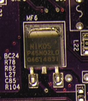
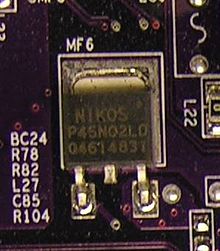 High-power N-channel field-effect transistor
The field-effect transistor (FET) is a transistor that relies on an electric field to control the shape and hence the conductivity of a channel of one type of charge carrier in a semiconductor material. FETs are sometimes called unipolar transistors to contrast their single-carrier-type operation with the dual-carrier-type operation of bipolar (junction) transistors (BJT). The concept of the FET predates the BJT, though it was not physically implemented until after BJTs due to the limitations of semiconductor materials and the relative ease of manufacturing BJTs compared to FETs at the time.
Contents
History
Main article: History of the transistorThe principle of field-effect transistors was first patented by Julius Edgar Lilienfeld in 1925 and by Oskar Heil in 1934, but practical semi-conducting devices (the JFET, junction gate field-effect transistor) were only developed much later after the transistor effect was observed and explained by the team of William Shockley at Bell Labs in 1947. The MOSFET (metal–oxide–semiconductor field-effect transistor), which largely superseded the JFET and had a more profound effect on electronic development, was first proposed by Dawon Kahng in 1960.[1]
Basic information
FETs are majority-charge-carrier devices. The device consists of an active channel through which majority charge carriers, electrons or holes, flow from the source to the drain. Source and drain terminal conductors are connected to semiconductor through ohmic contacts. The conductivity of the channel is a function of potential applied to the gate.[2][3]
The FET's three terminals are:[4]
- Source (S), through which the majority carriers enter the channel. Conventional current entering the channel at S is designated by IS.
- Drain (D), through which the majority carriers leave the channel. Conventional current entering the channel at D is designated by ID. Drain to Source voltage is VDS.
- Gate (G), the terminal that modulates the channel conductivity. By applying voltage to G, one can control ID.
More about terminals
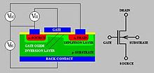
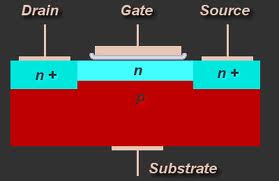
 Cross section of an n-type MOSFET
All FETs have gate, drain, and source terminals that correspond roughly to the base, collector, and emitter of BJTs. Most FETs also have a fourth terminal called the body, base, bulk, or substrate. This fourth terminal serves to bias the transistor into operation; it is rare to make non-trivial use of the body terminal in circuit designs, but its presence is important when setting up the physical layout of an integrated circuit. The size of the gate, length L in the diagram, is the distance between source and drain. The width is the extension of the transistor, in the diagram perpendicular to the cross section. Typically the width is much larger than the length of the gate. A gate length of 1 µm limits the upper frequency to about 5 GHz, 0.2 µm to about 30 GHz. Also, FET's Are less used than Bipolar transistors.
The names of the terminals refer to their functions. The gate terminal may be thought of as controlling the opening and closing of a physical gate. This gate permits electrons to flow through or blocks their passage by creating or eliminating a channel between the source and drain. Electrons flow from the source terminal towards the drain terminal if influenced by an applied voltage. The body simply refers to the bulk of the semiconductor in which the gate, source and drain lie. Usually the body terminal is connected to the highest or lowest voltage within the circuit, depending on type. The body terminal and the source terminal are sometimes connected together since the source is also sometimes connected to the highest or lowest voltage within the circuit, however there are several uses of FETs which do not have such a configuration, such as transmission gates and cascode circuits.
FET operation
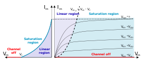 I–V characteristics and output plot of a JFET n-channel transistor.
The FET controls the flow of electrons (or electron holes) from the source to drain by affecting the size and shape of a "conductive channel" created and influenced by voltage (or lack of voltage) applied across the gate and source terminals (For ease of discussion, this assumes body and source are connected). This conductive channel is the "stream" through which electrons flow from source to drain.
In an n-channel depletion-mode device, a negative gate-to-source voltage causes a depletion region to expand in width and encroach on the channel from the sides, narrowing the channel. If the depletion region expands to completely close the channel, the resistance of the channel from source to drain becomes large, and the FET is effectively turned off like a switch. Likewise a positive gate-to-source voltage increases the channel size and allows electrons to flow easily.
Conversely, in an n-channel enhancement-mode device, a positive gate-to-source voltage is necessary to create a conductive channel, since one does not exist naturally within the transistor. The positive voltage attracts free-floating electrons within the body towards the gate, forming a conductive channel. But first, enough electrons must be attracted near the gate to counter the dopant ions added to the body of the FET; this forms a region free of mobile carriers called a depletion region, and the phenomenon is referred to as the threshold voltage of the FET. Further gate-to-source voltage increase will attract even more electrons towards the gate which are able to create a conductive channel from source to drain; this process is called inversion.
For either enhancement- or depletion-mode devices, at drain-to-source voltages much less than gate-to-source voltages, changing the gate voltage will alter the channel resistance, and drain current will be proportional to drain voltage (referenced to source voltage). In this mode the FET operates like a variable resistor and the FET is said to be operating in a linear mode or ohmic mode.[5][6]
If drain-to-source voltage is increased, this creates a significant asymmetrical change in the shape of the channel due to a gradient of voltage potential from source to drain. The shape of the inversion region becomes "pinched-off" near the drain end of the channel. If drain-to-source voltage is increased further, the pinch-off point of the channel begins to move away from the drain towards the source. The FET is said to be in saturation mode;[7] some authors refer to it as active mode, for a better analogy with bipolar transistor operating regions.[8][9] The saturation mode, or the region between ohmic and saturation, is used when amplification is needed. The in-between region is sometimes considered to be part of the ohmic or linear region, even where drain current is not approximately linear with drain voltage.
Even though the conductive channel formed by gate-to-source voltage no longer connects source to drain during saturation mode, carriers are not blocked from flowing. Considering again an n-channel device, a depletion region exists in the p-type body, surrounding the conductive channel and drain and source regions. The electrons which comprise the channel are free to move out of the channel through the depletion region if attracted to the drain by drain-to-source voltage. The depletion region is free of carriers and has a resistance similar to silicon. Any increase of the drain-to-source voltage will increase the distance from drain to the pinch-off point, increasing resistance due to the depletion region proportionally to the applied drain-to-source voltage. This proportional change causes the drain-to-source current to remain relatively fixed independent of changes to the drain-to-source voltage and quite unlike the linear mode operation. Thus in saturation mode, the FET behaves as a constant-current source rather than as a resistor and can be used most effectively as a voltage amplifier. In this case, the gate-to-source voltage determines the level of constant current through the channel.
Composition
The FET can be constructed from a number of semiconductors, silicon being by far the most common. Most FETs are made with conventional bulk semiconductor processing techniques, using the single crystal semiconductor wafer as the active region, or channel.
Among the more unusual body materials are amorphous silicon, polycrystalline silicon or other amorphous semiconductors in thin-film transistors or organic field effect transistors that are based on organic semiconductors and often apply organic gate insulators and electrode. The FETs are manufactured using variety of materials as silicon carbide(Sic),gallium arsenide(GaAs),gallium nitride(GaN),indium gallium arsenide(InGaAs). In June of 2011, IBM announced that it had successfully used graphene-based FETs in an integrated circuit.[10][11] These transistors are capable of a 100 GHz cutoff frequency, much higher than standard silicon FETs [12].
Types of field-effect transistors
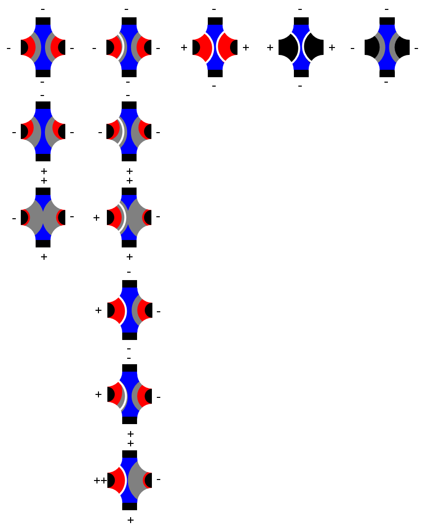
 Depletion-type FETs under typical voltages. JFET, poly-silicon MOSFET, double-gate MOSFET, metal-gate MOSFET, MESFET. depletion , electrons , holes , metal , insulator . Top=source, bottom=drain, left=gate, right=bulk. Voltages that lead to channel formation are not shown
The channel of a FET is doped to produce either an N-type semiconductor or a P-type semiconductor. The drain and source may be doped of opposite type to the channel, in the case of depletion mode FETs, or doped of similar type to the channel as in enhancement mode FETs. Field-effect transistors are also distinguished by the method of insulation between channel and gate. Types of FETs are:
- CNTFET (Carbon nanotube field-effect transistor)
- The DEPFET is a FET formed in a fully depleted substrate and acts as a sensor, amplifier and memory node at the same time. It can be used as an image (photon) sensor.
- The DGMOSFET is a MOSFET with dual gates.
- The DNAFET is a specialized FET that acts as a biosensor, by using a gate made of single-strand DNA molecules to detect matching DNA strands.
- The FREDFET (Fast Reverse or Fast Recovery Epitaxial Diode FET) is a specialized FET designed to provide a very fast recovery (turn-off) of the body diode.
- The HEMT (high electron mobility transistor), also called a HFET (heterostructure FET), can be made using bandgap engineering in a ternary semiconductor such as AlGaAs. The fully depleted wide-band-gap material forms the isolation between gate and body.
- The IGBT (insulated-gate bipolar transistor) is a device for power control. It has a structure akin to a MOSFET coupled with a bipolar-like main conduction channel. These are commonly used for the 200-3000 V drain-to-source voltage range of operation. Power MOSFETs are still the device of choice for drain-to-source voltages of 1 to 200 V.
- The ISFET (ion-sensitive field-effect transistor) used to measure ion concentrations in a solution; when the ion concentration (such as H+, see pH electrode) changes, the current through the transistor will change accordingly.
- The JFET (junction field-effect transistor) uses a reverse biased p-n junction to separate the gate from the body.
- The MESFET (Metal–Semiconductor Field-Effect Transistor) substitutes the p-n junction of the JFET with a Schottky barrier; used in GaAs and other III-V semiconductor materials.
- The MODFET (Modulation-Doped Field Effect Transistor) uses a quantum well structure formed by graded doping of the active region.
- The MOSFET (Metal–Oxide–Semiconductor Field-Effect Transistor) utilizes an insulator (typically SiO2) between the gate and the body.
- Depletion type MOSFET
There are two n-type island on p-type substrate. Between these two n regions there is a n-channel. The two n-regions form Source and Drain terminals. Gate terminal is to insulated layer of SiO2. There is conduction without any Gate voltage.
 D MOSFET
<[13]>
-
- Enhancement type MOSFET
Similar to Depletion type , but without n-channel. Hence for conduction there is requirement of some positive Gate voltage which attracts electrons from p-region which conducts from Source to Drain.
 E MOSFET
- The NOMFET is a Nanoparticle Organic Memory Field-Effect Transistor.[1]
- The OFET is an Organic Field-Effect Transistor using an organic semiconductor in its channel.
- The GNRFET is a Field-Effect Transistor that uses a graphene nanoribbon for its channel.
- The VeSFET (Vertical-Slit Field-Effect Transistor) is a square-shaped junction-less FET with a narrow slit connecting the source and drain at opposite corners. Two gates occupy the other corners, and control the current through the slit. [2] [3]
Advantages of FET
The main advantage of the FET is its high input resistance, on the order of 100M ohms or more. Thus, it is a voltage-controlled device, and shows a high degree of isolation between input and output. It is a unipolar device, depending only upon majority current flow. It is less noisy and is thus found in FM tuners for quiet reception. It is relatively immune to radiation. It exhibits no offset voltage at zero drain current and hence makes an excellent signal chopper. It typically has better thermal stability than a BJT.[4]
Disadvantages of FET
It has relatively low gain-bandwidth product compared to a BJT. The MOSFET has a drawback of being very susceptible to overload voltages, thus requiring special handling during installation.[16]
Uses
IGBTs see application in switching internal combustion engine ignition coils, where fast switching and voltage blocking capabilities are important.
The most commonly used FET is the MOSFET. The CMOS (complementary metal oxide semiconductor) process technology is the basis for modern digital integrated circuits. This process technology uses an arrangement where the (usually "enhancement-mode") p-channel MOSFET and n-channel MOSFET are connected in series such that when one is on, the other is off.
The fragile insulating layer of the MOSFET between the gate and channel makes it vulnerable to electrostatic damage during handling. This is not usually a problem after the device has been installed in a properly designed circuit.
In FETs electrons can flow in either direction through the channel when operated in the linear mode, and the naming convention of drain terminal and source terminal is somewhat arbitrary, as the devices are typically (but not always) built symmetrically from source to drain. This makes FETs suitable for switching analog signals between paths (multiplexing). With this concept, one can construct a solid-state mixing board, for example.
A common use of the FET is as an amplifier. For example, due to its large input resistance and low output resistance, it is effective as a buffer in common-drain (source follower) configuration.
See also
- Chemical field-effect transistor
- ISFET
- MOSFET
- FET amplifier
References
- ^ http://www.computerhistory.org/semiconductor/timeline/1960-MOS.html
- ^ http://commons.wikimedia.org/wiki/File:Basic_JFET.png
- ^ http://commons.wikimedia.org/wiki/File:Actual_JFET.png
- ^ a b Millman (1985). Electronic devices and circuits. Singapore: McGraw-Hill international book company. pp. 384–385. ISBN 0-07-Y85505-6.
- ^ C Galup-Montoro & Schneider MC (2007). MOSFET modeling for circuit analysis and design. London/Singapore: World Scientific. pp. 83. ISBN 981-256-810-7.
- ^ Norbert R Malik (1995). Electronic circuits: analysis, simulation, and design. Englewood Cliffs, NJ: Prentice Hall. pp. 315–316. ISBN 0-02-374910-5.
- ^ RR Spencer & Ghausi MS (2001). Microelectronic circuits. Upper Saddle River NJ: Pearson Education/Prentice-Hall. pp. 102. ISBN 0-201-36183-3.
- ^ A. S. Sedra and K.C. Smith (2004). Microelectronic circuits (Fifth Edition ed.). New York: Oxford. pp. 552. ISBN 0-19-514251-9.
- ^ PR Gray, PJ Hurst, SH Lewis & RG Meyer (2001). Analysis and design of analog integrated circuits (Fourth Edition ed.). New York: Wiley. pp. §1.5.2 p. 45. ISBN 0-471-32168-0.
- ^ http://www.physorg.com/news/2011-06-ibm-graphene-based-circuit.html
- ^ http://www.sciencemag.org/content/332/6035/1294
- ^ http://arxiv.org/ftp/arxiv/papers/1002/1002.3845.pdf
- ^ >{http://commons.wikimedia.org/wiki/File:MOSFET2.jpg}<
- ^ >{http://commons.wikimedia.org/wiki/File:MOSFET4.jpg}<
- ^ Robert Boylestad (2004). Electronic devices and circuit theory. New Delhi: Prentice Hall India.
- ^ Allen Mottershead (2004). Electronic devices and circuits. New Delhi: Prentice-Hall of India.
External links
- PBS The Field Effect Transistor
- Junction Field Effect Transistor
- The Enhancement Mode MOSFET
- CMOS gate circuitry
- Winning the Battle Against Latchup in CMOS Analog Switches
- Nanotube FETs at IBM Research
- Field Effect Transistors in Theory and Practice
- The Field Effect Transistor as a Voltage Controlled Resistor
Transistor amplifiers  Bipolar junction transistor: Common emitter • Common collector • Common base
Field-effect transistor: Common source • Common drain • Common gate
Multiple transistors: Darlington transistor • Sziklai pair • Cascode • Long-tailed pair
Electronic components Semiconductors Avalanche diode • Barretter • Darlington transistor • DIAC • Diode • Field-effect transistor (FET) • Insulated-gate bipolar transistor (IGBT) • JFET • Light-emitting diode (LED) • Memristor • MOSFET • Photodetector • PIN diode • Silicon-controlled rectifier (SCR) • Thyristor • Transistor • TRIAC • Unijunction transistor (UJT) • Zener diodeVacuum tubes Vacuum tubes (RF) Backward wave oscillator (BWO) • Cavity magnetron • Crossed-field amplifier • Gyrotron • Inductive output tube (IOT) • Klystron • Maser • Traveling-wave tubeAdjustable Passive Connector (Electrical power, Baseband, RF) • Ferrite • Fuse • Resettable fuse • Resistor (Thermistor) • TransformerReactive Categories:- Transistor types


Wikimedia Foundation. 2010.