- Depletion region
-
In semiconductor physics, the depletion region, also called depletion layer, depletion zone, junction region or the space charge region, is an insulating region within a conductive, doped semiconductor material where the mobile charge carriers have diffused away, or have been forced away by an electric field. The only elements left in the depletion region are ionized donor or acceptor impurities.
The 'depletion region' is so named because it is formed from a conducting region by removal of all free charge carriers, leaving none to carry a current. Understanding the depletion region is key to explaining modern semiconductor electronics: diodes, bipolar junction transistors, field-effect transistors, and variable capacitance diodes all rely on depletion region phenomena.
The following discussion is limited to the p-n junction and the MOS capacitor, but depletion regions arise in all the devices mentioned above.
Contents
Formation of depletion region in a P-N junction
 Top: pn junction before diffusion; Bottom: After equilibrium is reached
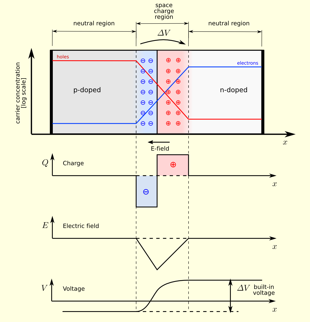
 Top: hole and electron concentrations through the junction; Second from top: charge densities; Third: electric field; Bottom: electric potential
A depletion region forms instantaneously across a P-N junction. It is most easily described when the junction is in thermal equilibrium or in a steady state: in both of these cases the properties of the system do not vary in time; they have been called dynamic equilibrium.[1] , [2]
Electrons and holes diffuse into regions with lower concentrations of electrons and holes, much as ink diffuses into water until it is uniformly distributed. By definition, N-type semiconductor has an excess of free electrons compared to the P-type region, and P-type has an excess of holes compared to the N-type region. Therefore when N-doped and P-doped pieces of semiconductor are placed together to form a junction, electrons migrate into the P-side and holes migrate into the N-side. Departure of an electron from the N-side to the P-side leaves a positive donor ion behind on the N-side, and likewise the hole leaves a negative acceptor ion on the P-side.
Following transfer, the diffused electrons come into contact with holes on the P-side and are eliminated by recombination. Likewise for the diffused holes on the N-side. The net result is the diffused electrons and holes are gone, leaving behind the charged ions adjacent to the interface in a region with no mobile carriers (called the depletion region). The uncompensated ions are positive on the N side and negative on the P side. This creates an electric field that provides a force opposing the continued exchange of charge carriers. When the electric field is sufficient to arrest further transfer of holes and electrons, the depletion region has reached its equilibrium dimensions. Integrating the electric field across the depletion region determines what is called the built-in voltage (also called the junction voltage or barrier voltage or contact potential).
- Mathematically speaking, charge transfer in semiconductor devices is due both to conduction driven by the electric field (drift) and by diffusion. For a P-type region, where holes conduct with electrical conductivity σ and diffuse with diffusion constant D, the net current density is given by
- with q the elementary charge (1.6×10⁻¹⁹ coulomb) and p the hole density (number per unit volume). Conduction forces the holes along the direction of the electric field. Diffusion moves the carriers in the direction of decreasing concentration, so for holes a negative current results for a positive density gradient. (If the carriers are electrons, we replace the hole density p by the negative of the electron density n; in some cases, both electrons and holes must be included.) When the two current components balance, as in the pn-junction depletion region at dynamic equilibrium, the current is zero due to the Einstein relation, which relates D to σ.
(1) Under reverse bias (P negative with respect to N), the potential drop (i.e., voltage) across the depletion region increases. This widens the depletion region, which increases the drift component of current and decreases the diffusion component. In this case the net current is leftward in the figure of the pn junction. The carrier density then is small and only a very small reverse saturation current flows.
(2) Forward bias (P positive with respect to N) narrows the depletion region and lowers the barrier to carrier injection. The diffusion component of the current greatly increases and the drift component decreases. In this case the net current is rightward in the figure of the pn junction. The carrier density is large (it varies exponentially with the applied bias voltage), making the junction conductive and allowing a large forward current.[3] The mathematical description of the current is provided by the Shockley diode equation. The low current conducted under reverse bias and the large current under forward bias is an example of rectification.
Formation of depletion region in an MOS capacitor
 Metal–oxide–semiconductor structure on P-type silicon
Another example of a depletion region occurs in the MOS capacitor. It is shown in the figure to the right, for a P-type substrate. Suppose that the semiconductor initially is charge neutral, with the charge due to holes exactly balanced by the negative charge due to acceptor doping impurities. If a positive voltage now is applied to the gate, which is done by introducing positive charge Q to the gate, then some positively charged holes in the semiconductor nearest the gate are repelled by the positive charge on the gate, and exit the device through the bottom contact. They leave behind a depleted region that is insulating because no mobile holes remain; only the immobile, negatively charged acceptor impurities. The greater the positive charge placed on the gate, the more positive the applied gate voltage, and the more holes that leave the semiconductor surface, enlarging the depletion region. (In this device there is a limit to how wide the depletion width may become. It is set by the onset of an inversion layer of carriers in a thin layer, or channel, near the surface. The above discussion applies for positive voltages low enough that an inversion layer does not form.)
If the gate material is polysilicon of opposite type to the bulk semiconductor, then a spontaneous depletion region forms if the gate is electrically shorted to the substrate, in much the same manner as described for the pn-junction above.
Depletion width
Depletion width describes the width of the depletion region in a semiconductor, particularly in geometries that are one-dimensional, like the pn-junction and MOS capacitor. The width of the depletion region is governed by the principle of charge neutrality. Two examples follow:
Depletion width in pn-junction
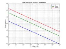 The total width of the depletion region is a function of applied reverse-bias and impurity concentration
The principle of charge neutrality says the sum of positive charges must equal the sum of negative charges:
-
-
 ,
,
-
where n and p are the number of free electrons and holes, and
 and
and  are the number of ionized donors and acceptors, respectively. If we assume full ionization and that n,p < < ND,NA, then:
-
-
 .
.
-
This condition ensures that the net negative acceptor charge exactly balances the net positive donor charge. The total depletion width in this case is the sum w = wN + wP. A full derivation for the depletion width is presented in reference.[4] This derivation is based on solving the Poisson equation in one dimension – the dimension normal to the metallurgical junction. The electric field is zero outside of the depletion width (seen in above figure) and therefore Gauss’s law implies that the charge density in each region balance – as shown by the first equation in this sub-section. Treating each region separately and substituting the charge density for each region into the Poisson equation eventually leads to a result for the depletion width. This result for the depletion width is:
![W \approx \left[ \frac{2K_s\epsilon_0}{q} \left(\frac{N_A + N_D}{N_A N_D}\right) \left(V_{bi} - V\right)\right]^\frac{1}{2}](5/c15683a978f86234571e7b4b1e210fc7.png)
where Ks is the semiconductor dielectric permitivity, Vbi is the built-in voltage, and V is the applied bias. The depletion region is not symmetrically split between the n and p regions - it will tend towards the lightly doped side.[5] A more complete analysis would take into account that there are still some carriers near the edges of the depletion region.[6] This leads to an additional -2kT/q term in the last set of parentheses above.
Depletion width in MOS capacitor
Again, the governing principle is charge neutrality. Let us assume a P-type substrate. If positive charge Q is placed on the gate, then holes are depleted to a depth w sufficient to expose sufficient negative acceptors to exactly balance the gate charge. Supposing the dopant density to be NA acceptors per unit volume, then charge neutrality requires the depletion width w to satisfy the relationship:
If the depletion width becomes wide enough, then electrons appear in a very thin layer at the semiconductor-oxide interface, called an inversion layer because they are oppositely charged to the holes that prevail in a P-type material. When an inversion layer forms the depletion width ceases to expand with increase in gate charge Q. In this case neutrality is achieved by attracting more electrons into the inversion layer. In the MOSFET this inversion layer is referred to as the channel.
Electric field in depletion layer and band bending
Associated with the depletion layer is an effect known as band bending. This occurs because the electric field in the depletion layer varies linearly in space from its (maximum) value Em at the gate to zero at the edge of the depletion width:[7]
where A is the gate area,
 = 8.854×10⁻¹² F/m, F is the farad and m is the meter. This linearly-varying electric field leads to an electrical potential that varies quadratically in space. The energy levels, or energy bands, bend in response to this potential.
See also
- Capacitance voltage profiling
- Metal–oxide–semiconductor structure
- Semiconductor diodes
References
- ^ Robert H. Bishop (2002). The Mechatronics Handbook. CRC Press. ISBN 0849300665. http://books.google.com/books?id=Q8zNV6AIvQ8C&pg=PT512&dq=depletion-region+called+because+mobile+charge&as_brr=3&sig=b84Bgy5mwkyY51uQKiYqEO1XqyI.
- ^ John E. Ayers (2003). Digital Integrated Circuits: Analysis and Design. CRC Press. ISBN 084931951X. http://books.google.com/books?id=QHtalNXHKbsC&pg=PA62&dq=thermal-equilibrium+depletion-region&as_brr=3&sig=5kOh5UaxuMfxRE-wi_BKcpk8iaU#PPA61,M1.
- ^ Sung-Mo Kang and Yusuf Leblebici (2002). CMOS Digital Integrated Circuits Analysis & Design. McGraw–Hill Professional. ISBN 0072460539. http://books.google.com/books?id=l1XyQ7RJ36cC&pg=PA90&dq=mos-structure+depletion-region&as_brr=3&sig=DgGIDCk8aBFKm6fIBYnO6R1Q5zg.
- ^ Pierret, Robert F. (1996). Semiconductor Device Fundamentals. pp. 209 to 216. http://www.amazon.com/Semiconductor-Device-Fundamentals-Robert-Pierret/dp/0201543931.
- ^ Sasikala, B; Afzal Khan, S. Pooranchandra, B. Sasikala (2005). Introduction to Electrical , Electronics and Communication Engineering. Firewall Media. ISBN 9788170086390.
- ^ Kittel, C; Kroemer, H. (1980). Thermal Physics. W. H. Freeman. ISBN 0716710889.
- ^ Wayne M. Saslow (2002). Electricity, Magnetism, and Light. Elsevier. ISBN 0126194556.
Categories:- Semiconductor structures


Wikimedia Foundation. 2010.