- Molecular beam epitaxy
-
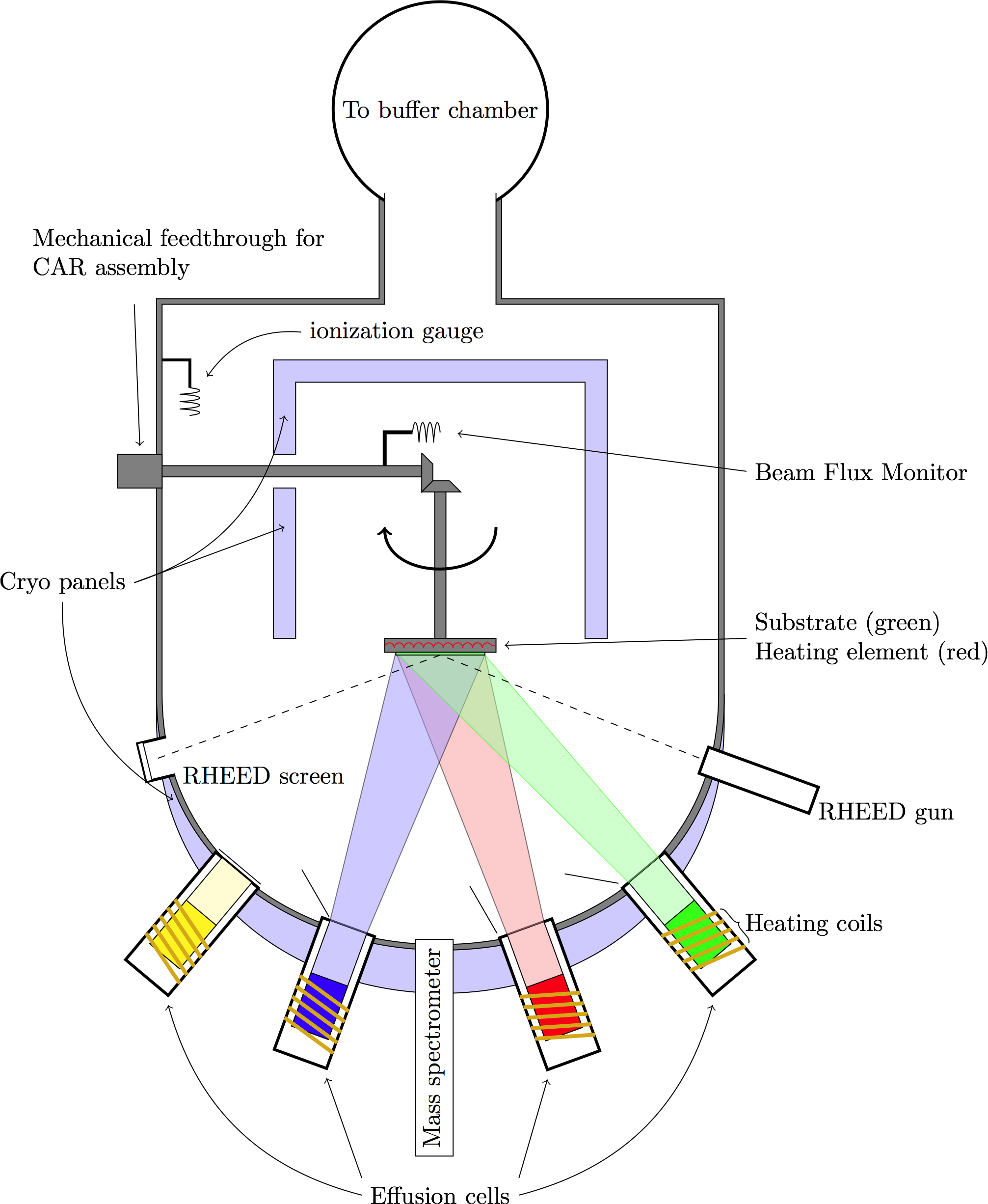
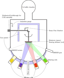 A simple sketch showing the main components and rough layout and concept of the main chamber in a Molecular Beam Epitaxy system
Molecular beam epitaxy (MBE) is one of several methods of depositing single crystals. It was invented in the late 1960s at Bell Telephone Laboratories by J. R. Arthur and Alfred Y. Cho.[1]
Contents
Method
Molecular beam epitaxy takes place in high vacuum or ultra-high vacuum (10−8 Pa). The most important aspect of MBE is the slow deposition rate (typically less than 1000 nm per hour), which allows the films to grow epitaxially. The slow deposition rates require proportionally better vacuum to achieve the same impurity levels as other deposition techniques.
In solid-source MBE, ultra-pure elements such as gallium and arsenic are heated in separate quasi-Knudsen effusion cells until they begin to slowly sublimate. The gaseous elements then condense on the wafer, where they may react with each other. In the example of gallium and arsenic, single-crystal gallium arsenide is formed. The term "beam" means that evaporated atoms do not interact with each other or vacuum chamber gases until they reach the wafer, due to the long mean free paths of the atoms.
During operation, reflection high energy electron diffraction (RHEED) is often used for monitoring the growth of the crystal layers. A computer controls shutters in front of each furnace, allowing precise control of the thickness of each layer, down to a single layer of atoms. Intricate structures of layers of different materials may be fabricated this way. Such control has allowed the development of structures where the electrons can be confined in space, giving quantum wells or even quantum dots. Such layers are now a critical part of many modern semiconductor devices, including semiconductor lasers and light-emitting diodes.
In systems where the substrate needs to be cooled, the ultra-high vacuum environment within the growth chamber is maintained by a system of cryopumps, and cryopanels, chilled using liquid nitrogen or cold nitrogen gas to a temperature close to 77 Kelvin (−196 degrees Celsius). Cryogenic temperatures act as a sink for impurities in the vacuum, so vacuum levels need to be several orders of magnitude better to deposit films under these conditions. In other systems, the wafers on which the crystals are grown may be mounted on a rotating platter which can be heated to several hundred degrees Celsius during operation.
Molecular beam epitaxy is also used for the deposition of some types of organic semiconductors. In this case, molecules, rather than atoms, are evaporated and deposited onto the wafer. Other variations include gas-source MBE, which resembles chemical vapor deposition.
ATG instability
The ATG (Asaro-Tiller-Grinfeld) instability, also known as the Grinfeld instability, is an elastic instability often encountered during molecular beam epitaxy. If there is a mismatch between the lattice sizes of the growing film and the supporting crystal, elastic energy will be accumulated in the growing film. At some critical height, the free energy of the film can be lowered if the film breaks into isolated islands, where the tension can be relaxed laterally. The critical height depends on Young's moduli, mismatch size, and surface tensions.
Some applications for this instability have been researched, such as the self-assembly of quantum dot. This community uses the name of Stranski–Krastanov growth for ATG.
See also
- Colin P. Flynn
- Arthur Gossard
- High electron mobility transistor (HEMT)
- Heterojunction bipolar transistor
- Herbert Kroemer
- Quantum cascade laser
- Solar cell
- Ben G. Streetman
- Wetting layer
Notes
- ^ Cho, A. Y.; Arthur, J. R.; Jr (1975). "Molecular beam epitaxy". Prog. Solid State Chem. 10: 157–192. doi:10.1016/0079-6786(75)90005-9.
References
- Jaeger, Richard C. (2002). "Film Deposition". Introduction to Microelectronic Fabrication. Upper Saddle River: Prentice Hall. ISBN 0-201-44494-7.
- McCray, W.P. (2007). "MBE Deserves a Place in the History Books". Nature Nanotechnology 2 (5): 259–261. Bibcode 2007NatNa...2..259M. doi:10.1038/nnano.2007.121. http://www.nature.com/nnano/journal/v2/n5/abs/nnano.2007.121.html.
- Shchukin, Vitaliy A.; Dieter Bimberg (1999). "Spontaneous ordering of nanostructures on crystal surfaces". Reviews of Modern Physics 71 (4): 1125–1171. Bibcode 1999RvMP...71.1125S. doi:10.1103/RevModPhys.71.1125.
- Stangl, J.; V. Holý and G. Bauer (2004). "Structural properties of self-organized semiconductor nanostructures". Reviews of Modern Physics 76 (3): 725–783. Bibcode 2004RvMP...76..725S. doi:10.1103/RevModPhys.76.725.
External links
Categories:- Semiconductor growth
- Thin film deposition
Wikimedia Foundation. 2010.