- Heterojunction bipolar transistor
-
The heterojunction bipolar transistor (HBT) is a type of bipolar junction transistor (BJT) which uses differing semiconductor materials for the emitter and base regions, creating a heterojunction. The HBT improves on the BJT in that it that can handle signals of very high frequencies, up to several hundred GHz. It is commonly used in modern ultrafast circuits, mostly radio-frequency (RF) systems, and in applications requiring a high power efficiency, such as RF power amplifiers in cellular phones. The idea of employing a heterojunction is as old as the conventional BJT, dating back to a patent from 1951[1].
Contents
Materials
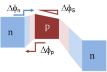
 Bands in graded heterojunction npn bipolar transistor. Barriers indicated for electrons to move from emitter to base, and for holes to be injected backward from base to emitter; Also, grading of bandgap in base assists electron transport in base region; Light colors indicate depleted regions
The principal difference between the BJT and HBT is in the use of differing semiconductor materials for the emitter and base regions, creating a heterojunction. The effect is to limit the injection of holes from the base into the emitter region, since the potential barrier in the valence band is higher than in the conduction band. Unlike BJT technology, this allows a high doping density to be used in the base, reducing the base resistance while maintaining gain. The efficiency of the heterojunction is measured by the Kroemer factor[2], named after Herbert Kroemer who was awarded a Nobel Prize for his work in this field in 2000 at the University of California, Santa Barbara.
Materials used for the substrate include silicon, gallium arsenide, and indium phosphide, while silicon / silicon-germanium alloys, aluminium gallium arsenide / gallium arsenide, and indium phosphide / indium gallium arsenide are used for the epitaxial layers. Wide-bandgap semiconductors are especially promising, e.g. gallium nitride and indium gallium nitride.
In SiGe graded heterostructure transistors, the amount of germanium in the base is graded, making the bandgap narrower at the collector than at the emitter. That tapering of the bandgap leads to a field-assisted transport in the base, which speeds transport through the base and increases frequency response.
Fabrication
Due to the need to manufacture HBT devices with extremely high-doped thin base layers, molecular beam epitaxy is principally employed. In addition to base, emitter and collector layers, highly doped layers are deposited on either side of collector and emitter to facilitate an ohmic contact, which are placed on the contact layers after exposure by photolithography and etching. The contact layer underneath the collector, named subcollector, is an active part of the transistor.
Other techniques are used depending on the material system. IBM and others use UHV CVD for SiGe; other techniques used include MOVPE for III-V systems.
Limits
A pseudomorphic heterojunction bipolar transistor developed at the University of Illinois at Urbana-Champaign, built from indium phosphide and indium gallium arsenide and designed with compositionally graded collector, base and emitter, was demonstrated to cut off at a speed of 710 gigahertz.[3][4]
Besides being record breakers in terms of speed, HBTs made of InP/InGaAs are ideal for monolithic optoelectronic integrated circuits. A PIN-type photo detector is formed by the base-collector-subcollector layers. The bandgap of InGaAs works well for detecting 1.55μm-wavelength infrared laser signals used in optical communication systems. Biasing the HBT to obtain an active device, a photo transistor with high internal gain is obtained. Among other HBT applications are mixed signal circuits such as analog-to-digital and digital-to-analog converters.
See also
References
- ^ W. Schockley: 'Circuit Element Utilizing Semiconductive Material', United States Patent 2,569,347, 1951.
- ^ The phototransistor effect: "The Kroemer factor is a function of the physical parameters of the materials making up the heterojunction, and can be expressed in the following way [formula given]"
- ^ Hafez et al, Appl. Phys. Lett. 87, 252109, 2005 doi:10.1063/1.2149510
- ^ Semiconductor Today
External links
- NCSR HBT at the Wayback Machine (archived April 4, 2008)
- HBT Optoelectronic Circuits developed in the Technion (15Mb, 230p)
- New Material Structure Produces World's Fastest Transistor 604 GHz Early 2005
Categories:- Microwave technology
- Terahertz technology
- Transistor types
Wikimedia Foundation. 2010.
