- Microbolometer
-
A microbolometer is a specific type of bolometer used as a detector in a thermal camera. Infrared radiation with wavelengths between 7.5-14 μm strikes the detector material, heating it, and thus changing its electrical resistance. This resistance change is measured and processed into temperatures which can be used to create an image. Unlike other types of infrared detecting equipment, microbolometers do not require cooling.
Contents
Theory of operation
A microbolometer is an uncooled thermal sensor. Previous high resolution thermal sensors required exotic and expensive cooling methods including stirling cycle coolers and liquid nitrogen coolers. These methods of cooling made early thermal imagers expensive to operate and unwieldy to move. Also, older thermal imagers required a cool down time in excess of 10 minutes before being usable.
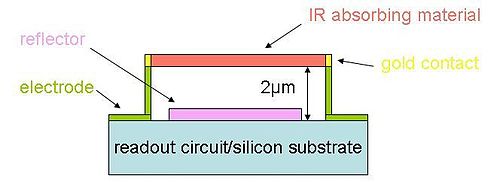
A microbolometer consists of an array of pixels, each pixel being made up of several layers. The cross-sectional diagram shown in Figure 1 provides a generalized view of the pixel. Each company that manufactures microbolometers has their own unique procedure for producing them and they even use a variety of different absorbing materials. In this example the bottom layer consists of a silicon substrate and a readout integrated circuit (ROIC). Electrical contacts are deposited and then selectively etched away. A reflector, for example, a titanium mirror, is created beneath the IR absorbing material. Since some light is able to pass through the absorbing layer, the reflector redirects this light back up to ensure the greatest possible absorption, hence allowing a stronger signal to be produced. Next, a sacrificial layer is deposited so that later in the process a gap can be created to thermally isolate the IR absorbing material from the ROIC. A layer of absorbing material is then deposited and selectively etched so that the final contacts can be created. To create the final bridge like structure shown in Figure 1, the sacrificial layer is removed so that the absorbing material is suspended approximately 2 μm above the readout circuit. Because microbolometers do not undergo any cooling, the absorbing material must be thermally isolated from the bottom ROIC and the bridge like structure allows for this to occur. After the array of pixels is created the microbolometer is encapsulated under a vacuum to increase the longevity of the device. In some cases the entire fabrication process is done without breaking vacuum.The quality of images created from microbolometers has continued to increase. The microbolometer array is commonly found in two sizes, 320×240 pixels or less expensive 160×120 pixels. Current technology has led to the production of devices with 640×480 or 1024x768 pixels. There has also been a decrease in the individual pixel dimensions. The pixel size was typically 45 μm in older devices and has been decreased to 17 μm in current devices. As the pixel size is decreased and the number of pixels per unit area is increased proportionally, an image with higher resolution is created.
Detecting material properties
There is a wide variety of materials that are used for the detector element in microbolometers. A main factor in dictating how well the device will work is the devices responsivity. Responsivity is the ability of the device to convert the incoming radiation into an electrical signal. Detector material properties influence this value and thus several main material properties should be investigated: TCR, 1/f Noise, and Resistance.
Temperature coefficient of resistance
The material used in the detector must demonstrate large changes in resistance as a result of minute changes in temperature. As the material is heated, due to the incoming infrared radiation, the resistance of the material decreases. This is related to the material's temperature coefficient of resistance (TCR) specifically its negative temperature coefficient. Industry currently manufactures microbolometers that contain materials with TCRs near -2%. Although many materials exist that have far higher TCRs, there are several other factors that need to be taken into consideration when producing optimized microbolometers.
1/f noise
1/f noise, like other noises, causes a disturbance that affects the signal and that may distort the information carried by the signal. Changes in temperature across the absorbing material are determined by changes in the bias current or voltage flowing through the detecting material. If the noise is large then small changes that occur may not be seen clearly and the device is useless. Using a detector material that has a minimum amount of 1/f noise allows for a clearer signal to be maintained between IR detection and the output that is displayed. Detector material must be tested to assure that this noise does not significantly interfere with signal.
Resistance
Using a material that has low room temperature resistance is also important. Lower resistance across the detecting material mean less power will need to be used. Also, there is a relationship between resistance and noise, the higher the resistance the higher the noise. Thus, for easier detection and to satisfy the low noise requirement, resistance should be low.
Detecting materials
The two most commonly used IR radiation detecting materials in microbolometers are amorphous silicon and vanadium oxide. Much research has been done to test other materials feasibility to be used as a detecting material. Other materials that have been investigated include: Ti, YBaCuO, GeSiO, poly SiGe, BiLaSrMnO and a protein based cytochrome C and bovine serum albumin.
Amorphous Si (a-Si) works well mainly because it can easily be integrated into the CMOS fabrication process. To create the layered structure and patterning, the CMOS fabrication process can be used but it requires temperatures to stay below 200˚C on average. A problem with some potential materials is that to create the desirable properties their deposition temperatures may be too high although this is not a problem for a-Si thin films. a-Si also possesses reasonable values for TCR, 1/f noise and resistance when the deposition parameters are optimized.
Vanadium oxide thin films may also be integrated into the CMOS fabrication process although not as easily as a-Si for temperature reasons. Deposition at high temperatures and performing post-annealing allows for the production of films with superior properties although acceptable films can still be made subsequently fulfilling the temperature requirements. VO2 has low resistance but undergoes a metal-insulator phase change near 67oC and also has a lower value of TCR. On the other hand, V2O5 exhibits high resistance and also high TCR. Many phases of VOx exist although it seems that x≈1.8 has become the most popular for microbolometer applications.
Active vs passive microbolometers
Most microbolometers contain a temperature sensitive resistor which makes them a passive electronic device. In 1994 one company, Electro-Optic Sensor Design (EOSD), began looking into producing microbolometers that used a thin film transistor (TFT), which is a special kind of field effect transistor. The main change in these devices would be the addition of a gate electrode. Although the main concepts of the devices are similar, using this design allows for the advantages of the TFT to be utilized. Some benefits include tuning of the resistance and activation energy and the reduction of periodic noise patterns. As of 2004 this device was still being tested and was not used in commercial IR imaging.
Advantages
- Collect the light in the 7.5 μm to 14 μm spectral band. This spectral band provides a better penetration through smoke, smog, dust, water vapor etc. because the wavelength is much longer than visible light in the 0.4 to 0.7 μm spectral band.
- They are small and lightweight. For applications requiring relatively short ranges, the physical dimensions of the camera are even smaller. This property enables, for example, the mounting of uncooled microbolometer thermal imagers on helmets.
- Provide real video output immediately after power on.
- Low power consumption relative to cooled detector thermal imagers.
- Very long MTBF.
- Less expensive compared to cameras based on cooled detectors.
Disadvantages
- Less sensitive than cooled detector thermal imagers.
- Cannot be used for multispectral or high-speed infrared applications.
- Infrared radiation does not travel through common glass windows and therefore microbolometers can not be used to produce images if they are behind a standard glass window.
Performance limits
The sensitivity is partly limited by the thermal conductance of the pixel. The speed of response is limited by the thermal heat capacity divided by the thermal conductance. Reducing the heat capacity increases the speed but also increases statistical mechanical thermal temperature fluctuations (noise). Increasing the thermal conductance raises the speed, but decreases sensitivity.
Origins
The microbolometer technology was originally developed by Honeywell starting in the late 70's as a classified contract for the US Department of Defense. The US Government declassified the technology in 1992. After declassification Honeywell licensed their technology to several manufacturers.
Manufacturers of microbolometer arrays
- Fluke Corporation
- BAE Systems
- Raytheon
- L-3 Communications Infrared Products (Company Web Site)
- DRS Technologies
- FLIR Systems (Company Web Site)
- Opgal Optronics Ltd (Company Web Site)
- Vumii Imaging(Company Web Site)
- InfraredVision Technologies Corporation
- NEC
- Institut National d'Optique (INO) (Company Web Site)
- Honeywell (Manufactured for Infrared Solutions)
- ULIS-IR (Company Web Site)
- SCD - SemiConductor devices
- Lockheed Martin - Santa Barbara Focalplane (Company Web Site)
- Qioptiq Ltd. UK (Company Web Site)
References
- Wang, Hongchen; Xinjian Yi, Jianjun Lai and Yi Li (31 January 2005). "Fabricating Microbolometer Array on Unplanar Readout Integrated Circuit". International Journal of Infrared and Millimeter Waves 26 (5): 751–762. Bibcode 2005IJIMW..26..751W. doi:10.1007/s10762-005-4983-8.
- LETI. "Microbolometers". http://www-leti.cea.fr/scripts/home/publigen/content/templates/show.asp?P=300&L=EN&SYNC=Y. Retrieved 2007-12-03.[dead link]
- Deb, K.K; Ionescu, A.C., Li, C. (August 2000). "Protein-based thin films: A new high-TCR material". Sensors (Peterborough, NH: Advanstar Communications) 17 (8): 52–55. http://archives.sensorsmag.com/articles/0800/52/index.htm. Retrieved 2007-12-03.
- Kumar, R.T. Rajendra; B. Karunagarana, D. Mangalaraja,, Sa.K. Narayandassa, P. Manoravib, M. Josephb, Vishnu Gopalc, R.K. Madariac, J.P. Singhc (18 March 2003). "Room temperature deposited vanadium oxide thin films for uncooled infrared detectors". Materials Research Bulletin 38 (7): 1235–1240. doi:10.1016/S0025-5408(03)00118-1.
- Liddiard, Kevin C. (2004). The active microbolometer: a new concept in infrared detection. "Proceedings of SPIE". Proceedings of SPIE (Bellingham, WA: SPIE) 5274: 227–238. doi:10.1117/12.530832.
Categories:- Radiometry
- Particle detectors
- Image sensors
- Infrared imaging
Wikimedia Foundation. 2010.


