- Micro contact printing
-
Microcontact printing (or μCP) is a form of soft lithography that uses the relief patterns on a master Polydimethylsiloxane (PDMS) stamp to form patterns of self-assembled monolayers (SAMs) of ink on the surface of a substrate through conformal contact. Its applications are wide ranging including microelectronics, surface chemistry and cell biology.
Contents
History
Both lithography and stamp printing have been around for centuries. However, the combination of the two gave rise to the method of microcontact printing. The method was first introduced by George M. Whitesides and Amit Kumar at Harvard University. Since its inception many methods of soft lithography have been explored.
Procedure
Preparing the Master
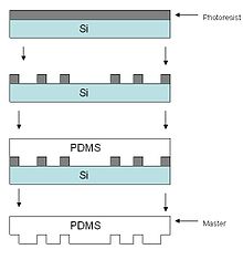
Creation of the master, or template, is done using traditional photolithography techniques. The master is typically created on silicon, but can be done on any solid patterned surface. Photoresist is applied to the surface and patterned by a photomask and UV light. The master is then baked, developed and cleaned before use. In typical processes the photoresist is usually kept on the wafer to be used as a topographic template for the stamp. However, the unprotected silicon regions can be etched, and the photoresist stripped, which would leave behind a patterned wafer for creating the stamp. This method is more complex but creates a more stable template.
Creating the PDMS Stamp
After fabrication the master is placed in a walled container, typically a petri dish, and the stamp is poured over the master.
The PDMS stamp, in most applications, is a 10:1 ratio of silicone elastomer and a silicone elastomer curing agent. This mixture consists of a short hydrosilane crosslinker that contains a catalyst made from a platinum complex. After pouring, the PDMS is cured at elevated temperatures to create a solid polymer with elastomeric properties. The stamp is then peeled off and cut to the proper size. The stamp replicates the opposite of the master. Elevated regions of the stamp correspond to indented regions of the master.
Inking the Stamp
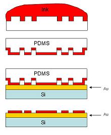
Inking of the stamp occurs through the application of a thiol solution either by immersion or coating the stamp with a Q-tip. The highly hydrophobic PDMS material allows the ink to be diffused into the bulk of the stamp, which means the thiols reside not only on the surface, but also in the bulk of the stamp material. This diffusion into the bulk creates an ink reservoir for multiple prints. The stamp is let dry until no liquid is visible to the eye and an ink reservoir is created.
Applying the Stamp to the Substrate
Direct Contact
Applying the stamp to the substrate is easy and straightforward which is one of the main advantages of this process. The stamp is brought into physical contact with the substrate and the thiol solution is transferred to the substrate. The thiol is area-selectively transferred to the surface based on the features of the stamp. During the transfer the carbon chains of the thiol align with each other to create a hydrophobic self-assembling monolayer (SAM).
Other Application Techniques
Printing of the stamp onto the substrate, although not used as often, can also take place with a rolling stamp onto a planar substrate or a curved substrate with a planar stamp.
Advantages
Microcontact Printing has several advantages including:
- The simplicity and ease of creating patterns with micro-scale features
- Can be done in a traditional laboratory without the constant use of a cleanroom (cleanroom is needed only to create the master).
- Multiple stamps can be created from a single master
- Individual stamps can be used several times with minimal degradation of performance
- A cheaper technique for fabrication that uses less energy than conventional techniques
Technical Problems with Microcontact Printing
After this technique became popular various limitations and problems arose, all of which affected patterning and reproducibility.
Stamp Deformation
During direct contact one must be careful because the stamp can easily be physically deformed causing printed features that are different than the original stamp features. Horizontally stretching or compressing the stamp will cause deformations in the raised and recessed features. Also, applying too much vertical pressure on the stamp during printing can cause the raised relief features to flatten against the substrate. These deformations can yield submicron features even though the original stamp has a lower resolution.
Deformation of the stamp can occur during removal from the master and during the substrate contacting process. When the aspect ratio of the stamp is high buckling of the stamp can occur. When the aspect ratio is low roof collapse can occur
Substrate Contamination
During the curing process some fragments can potentially be left uncured and contaminate the process. When this occurs the quality of the printed SAM is decreased. When the ink molecules contain certain polar groups the transfer of these impurities is increased.
Shrinking/Swelling of the Stamp
During the curing process the stamp can potentially shrink in size leaving a difference in desired dimensions of the substrate patterning.
Swelling of the stamp may also occur. Most organic solvents induce swelling of the PDMS stamp. Ethanol in particular has a very small swelling effect, but many other solvents cannot be used for wet inking because of high swelling. Because of this the process is limited to apolar inks that are soluble in ethanol.
Ink Mobility
Ink diffusion from the PDMS bulk to the surface occurs during the formation of the patterned SAM on the substrate. This mobility of the ink can cause lateral spreading to unwanted regions. Upon the transfer this spreading can influence the desired pattern.
Applications
Depending on the type of ink used and the subsequent substrate the microcontact printing technique has many different applications
Micromachining
Microcontact printing has great applications in micromachining. For this application inking solutions commonly consist of a solution of alkanethiol.[1] This method uses metal substrates with the most common metal being gold. However, silver, copper, and palladium have been proven to work as well.
Once the ink has been applied to the substrate the SAM layer acts as a resist to common wet etching techniques allowing for the creation of high resolution patterning. The patterned SAMs layer is a step in a series of steps to create complex microstructures. For example, applying the SAM layer on top of gold and etching creates microstructures of gold. After this step etched areas of gold exposes the substrate which can further be etched using traditional anisotropic etch techniques. Because of the microcontact printing technique no traditional photolithography is needed to accomplish these steps.
Patterning Proteins
The patterning of proteins has helped the advancement of biosensors.,[2] cell biology research [3]., and tissue engineering.[4] Various proteins have been proven to be suitable inks and are applied to various substrates using the microcontact printing technique. Polylysine, immunoglobulin antibody, and different enzymes have been successfully placed onto surfaces including glass, polystyrene, and hydrophobic silicon.
Patterning Cells
Microcontact printing has been used to advance the understanding of how cells interact with substrates. This technique has helped improve the study of cell patterning that was not possible with traditional cell culture techniques.
Patterning DNA
Successful patterning of DNA has also been done using this technique.[5][6] The reduction in time and DNA material are the critical advantages for using this technique. The stamps were able to be used multiple times that were more homogeneous and sensitive than other techniques.
Technique Improvements
To help overcome the limitations set by the original technique several alternatives have been developed.
- High-Speed printing: Successful contact printing was done on a gold substrate with a contact time in the range of milliseconds. This printing time is three orders of magnitude shorter than the normal technique, yet successfully transformed the pattern. The process of contact was automated to achieve these speeds through a piezoelectric actuator. At these low contact times the surface spreading of thiol did not occur, greatly improving the pattern uniformity[3]
- Submerged Printing: By submerging the stamp in a liquid medium stability was greatly increased. By printing hydrophobic long-chain thiols underwater the common problem of vapor transport of the ink is greatly reduced. PDMS aspect ratios of 15:1 were achieved using this method, which was not accomplished before[4]
- Contact Inking: as opposed to wet inking this technique does not permeate the PDMS bulk. The ink molecules only contact the protruding areas of the stamp that are going to be used for the patterning. The absence of ink on the rest of the stamp reduces the amount of ink transferred through the vapor phase that can potentially affect the pattern. This is done by the direct contact of a feature stamp and a flat PDMS substrate that has ink on it.[[7]
- New Stamp Materials: In order to create uniform transfer of the ink the stamp needs to be both mechanically stable and also be able to create conformal contact well. These two characteristics are juxtaposed because high stability requires a high Young’s Modulus while efficient contact requires an increase in elasticity. A composite, thin PDMS stamp with a rigid back support has been used for patterning to help solve this problem.
General references
- Wilbur J.L. et al. (1996). Microcontact printing of self-assembled monolayers: applications in microfabrication.. Nanotechnology.
- Ruiz S.A., Chen C.S.. Microcontact Printing: A tool to pattern. Soft Matter year= 2007.
- Reinhoudt, Huskens (2009). Microcontact printing: limitations and achievements. Advanced Materials.
Footnotes
- ^ Wilbur, J.L. (1996). Microcontact printing of self-assembled monolayers: applications in microfabrication. Nanotechnology.
- ^ Gross, G.W., et al. (1995).
- ^ a b Chen, Mrksich, Huang, Whitesides,Ingber (1997). Science.
- ^ a b Bhatia, Balis, Yarmush and Toner (1999). FASEB J..
- ^ Lange, Benes, Kern, Horber, and Bernard (2004). Anal. Chem..
- ^ Thibault, Le Berre, Casimirius, Trevisiol, Francois, and Vieu (2005). Nanobiotechnol..
- ^ Libioulle, Bietsch, Schmid, Michel, Delamarche and Langmuir (1999).
Categories:- Lithography (microfabrication)
Wikimedia Foundation. 2010.


