- Direct and indirect band gaps
-
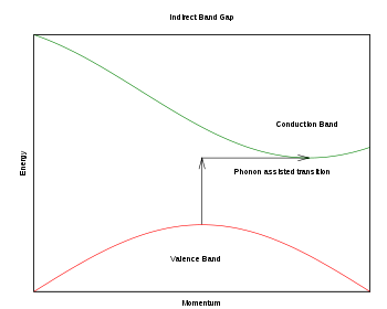
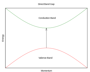
In semiconductor physics, the band gap of a semiconductor is always one of two types, a direct band gap or an indirect band gap. The band gap is called "direct" if the momentum of electrons and holes is the same in both the conduction band and the valence band; an electron can directly emit a photon. In an "indirect" gap, a photon cannot be emitted because the electron must pass through an intermediate state and transfer momentum to the crystal lattice. The minimal-energy state in the conduction band, and the maximal-energy state in the valence band, are each characterized by a certain crystal momentum (k-vector) in the Brillouin zone. If the k-vectors are the same, it is called a "direct gap". If they are different, it is called an "indirect gap".
 Energy vs. crystal momentum for a semiconductor with an indirect band gap, showing that an electron cannot shift from the lowest-energy state in the conduction band (green) to the highest-energy state in the valence band (red) without a change in momentum. Here, almost all of the energy comes from a photon (vertical arrow), while almost all of the momentum comes from a phonon (horizontal arrow).
 Energy vs. crystal momentum for a semiconductor with a direct band gap, showing that an electron can shift from the lowest-energy state in the conduction band (green) to the highest-energy state in the valence band (red) without a change in crystal momentum. Depicted is a transition in which a photon excites an electron from the valence band to the conduction band.
Contents
Implications for radiative recombination
See also: Radiative recombinationInteractions among electrons, holes, phonons, photons, and other particles are required to satisfy conservation of energy and crystal momentum (i.e., conservation of total k-vector). A photon with an energy near a semiconductor band gap has almost zero momentum. An important process is called radiative recombination, where an electron in the conduction band annihilates a hole in the valence band, releasing the excess energy as a photon. If the electron is near the bottom of the conduction band and the hole is near the top of the valence band (as is usually the case), this process is possible in a direct band gap semiconductor, but impossible in an indirect band gap one, because conservation of crystal momentum would be violated. For radiative recombination to occur in an indirect band gap material, the process must also involve the absorption or emission of a phonon, where the phonon momentum equals the difference between the electron and hole momentum. (It can also, instead, involve a crystallographic defect, which performs essentially the same role.) The involvement of the phonon makes this process much less likely to occur in a given span of time, which is why radiative recombination is far slower in indirect band gap materials than direct band gap ones. This is why light-emitting and laser diodes are almost always made of direct band gap materials, and not indirect band gap ones like silicon.
The fact that radiative recombination is slow in indirect band gap materials also means that, under most circumstances, radiative recombinations will be a small proportion of total recombinations, with most recombinations being non-radiative, taking place at point defects or at grain boundaries. However, if the excited electrons are prevented from reaching these recombination places, they have no choice but to eventually fall back into the valence band by radiative recombination. This can be done by creating a dislocation loop in the material. At the edge of the loop, the planes above and beneath the "dislocation disk" are pulled apart, creating a negative pressure, which raises the energy of the conduction band substantially, with the result that the electrons cannot pass this edge. Provided that the area directly above the dislocation loop is defect-free (no non-radiative recombination possible), the electrons will fall back into the valence shell by radiative recombination and thus emitting light. This is the principle on which "DELEDs" (Dislocation Engineered LEDs) are based.
Implications for light absorption
The exact reverse of radiative recombination is light absorption. For the same reason as above, light with a photon energy close to the band gap can penetrate much farther before being absorbed in an indirect band gap material than a direct band gap one (at least insofar as the light absorption is due to exciting electrons across the band gap).
This fact is very important for photovoltaics (solar cells). Silicon is the most common solar-cell material, despite the fact that it is indirect-gap and therefore does not absorb light very well. Silicon solar cells are typically hundreds of micrometres thick; if it was much thinner, much of the light (particularly in the infrared) would simply pass through. On the other hand, thin-film solar cells are made of direct band gap materials (such as CdTe or CIGS), which absorb the light in a much thinner region, and consequently can be made with a very thin active layer (often less than 1 micrometre thick).
The absorption spectrum of an indirect band gap material usually depends more on temperature than that of a direct material, because at low temperatures there are fewer phonons, and therefore it is less likely that a photon and phonon can be simultaneously absorbed to create an indirect transition. For example, silicon starts to transmit red light at liquid helium temperatures, because red photons do not have sufficient energy for an indirect process.
Formulas for absorption
A common and simple method for determining whether a band gap is direct or indirect uses absorption spectroscopy. By plotting certain powers of the absorption coefficient against photon energy, one can normally tell both what value the band gap has, and whether or not it is direct.
For a direct band gap, the absorption coefficient α is related to light frequency according to the following formula:[1][2]
 , with
where:
- α is the absorption coefficient, a function of light frequency
- ν is light frequency
- h is Planck's constant (hν is the energy of a photon with frequency ν)
 is reduced Planck's constant (
 )
)- Eg is the band gap energy
- A * is a certain frequency-independent constant, with formula above
 , where
  and
and  are the effective masses of the electron and hole, respectively (mr is called a "reduced mass")
- q is the elementary charge
- n is the (real) index of refraction
 is the vacuum permittivity
- xvc is a "matrix element", with units of length and typical value the same order of magnitude as the lattice constant.
This formula is valid only for light with photon energy larger, but not too much larger, than the band gap (more specifically, this formula assumes the bands are approximately parabolic), and ignores all other sources of absorption other than the band-to-band absorption in question, as well as the electrical attraction between the newly created electron and hole (see exciton). It is also invalid in the case that the direct transition is forbidden, or in the case that many of the valence band states are empty or conduction band states are full.[3]
On the other hand, for an indirect band gap, the formula is:[3]
where:
- Ep is the energy of the phonon that assists in the transition
- k is Boltzmann's constant
- T is the thermodynamic temperature
(This formula involves the same approximations mentioned above.)
Therefore, if a plot of hν versus α2 forms a straight line, it can normally be inferred that there is a direct band gap, measurable by extrapolating the straight line to the α = 0 axis. On the other hand, if a plot of hν versus α1 / 2 forms a straight line, it can normally be inferred that there is an indirect band gap, measurable by extrapolating the straight line to the α = 0 axis (assuming
 ).
).Other aspects
In some materials with an indirect gap, the value of the gap is negative. The top of the valence band is higher than the bottom of the conduction band in energy. Such materials are known as semimetals.
References
- ^ Optoelectronics, by E. Rosencher, 2002, equation (7.25).
- ^ Pankove has the same equation, but with an apparently different prefactor A * . However, in the Pankove version, the units / dimensional analysis appears not to work out.
- ^ a b J.I. Pankove, Optical Processes in Semiconductors. Dover, 1971.
External links
- B. Van Zeghbroeck's Principles of Semiconductor Devices at Electrical and Computer Engineering Department of University of Colorado at Boulder
Categories:- Electronic band structures
- Optoelectronics
Wikimedia Foundation. 2010.

