- Chemical-mechanical planarization
-
Chemical Mechanical Polishing/Planarization is a process of smoothing surfaces with the combination of chemical and mechanical forces. It can be thought of as a hybrid of chemical etching and free abrasive polishing.
Contents
Description
 functional principle of CMP
The process uses an abrasive and corrosive chemical slurry (commonly a colloid) in conjunction with a polishing pad and retaining ring, typically of a greater diameter than the wafer. The pad and wafer are pressed together by a dynamic polishing head and held in place by a plastic retaining ring. The dynamic polishing head is rotated with different axes of rotation (i.e., not concentric). This removes material and tends to even out any irregular topography, making the wafer flat or planar. This may be necessary in order to set up the wafer for the formation of additional circuit elements. For example, this might be necessary in order to bring the entire surface within the depth of field of a photolithography system, or to selectively remove material based on its position. Typical depth-of-field requirements are down to Angstrom levels for the latest 65 nm technology.
Working Principles
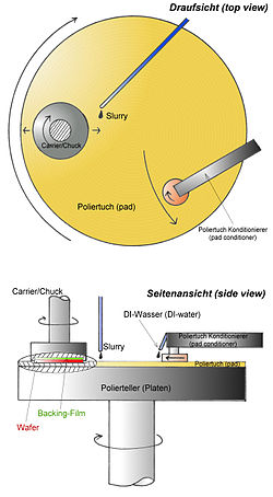
Typical CMP tools, such as the ones seen on the right, consist of a rotating and extremely flat platen which is covered by a pad. The wafer that is being polished is mounted upside-down in a carrier/spindle on a backing film. The retaining ring (Figure 1) keeps the wafer in the correct horizontal position. During the process of loading and unloading the wafer onto the tool, the wafer is held by vacuum by the carrier to prevent unwanted particles from building up on the wafer surface. A slurry introduction mechanism deposits the slurry on the pad, this is represented by the slurry supply in Figure 1. Both the platen and the carrier are then rotated and the carrier is kept oscillating as well; this can be better seen in the top view of Figure 2. A downward pressure/down force is applied to the carrier, pushing it against the pad; typically the down force is an average force, but local pressure is needed for the removal mechanisms. Down force depends on the contact area which, in turn, is dependent on the structures of both the wafer and the pad. Typically the pads have a roughness of 50µm; contact is made by asperities (which typically are the high points on the wafer) and, as a result, the contact area is only a fraction of the wafer area. In CMP, the mechanical properties of the wafer itself must be considered too. If the wafer has a slightly bowed structure, the pressure will be greater on the edges than it would on the center, which causes non-uniform polishing. In order to compensate for the wafer bow, pressure can be applied to the wafer’s backside which, in turn, will equalize the centre-edge differences. The pads used in the CMP tool should be rigid in order to uniformly polish the wafer surface. However, these rigid pads must be kept in alignment with the wafer at all times. Therefore, real pads are often just stacks of soft and hard materials that conform to wafer topography to some extent. Generally, these pads are made from porous polymeric materials with a pore size between 30-50µm, are consumed in the process, and must be regularly reconditioned. In most cases the pads are very much proprietary, and are usually referred to by their trademark names rather than their chemical or other properties.
Usage in semiconductor fabrication
Before about 1990 CMP was looked on as too "dirty" to be included in high-precision fabrication processes, since abrasion tends to create particles and the abrasives themselves are not without impurities. Since that time, the integrated circuit industry has moved from aluminium to copper conductors. This required the development of an additive patterning process, which relies on the unique abilities of CMP to remove material in a planar and uniform fashion and to stop repeatably at the interface between copper and oxide insulating layers (see Copper-based chips for details). Adoption of this process has made CMP processing much more widespread. In addition to aluminum and copper, CMP processes have been developed for polishing tungsten, silicon dioxide, and (recently) carbon nanotubes.[1]
Limitations of CMP
There are currently several limitations of CMP that appear during the polishing process requiring optimization of a new technology. In particular, an increase in the wafer metrology is required. In addition, it was discovered that CMP process has several potential defects including stress cracking, delaminating at weak interfaces, and corrosive attacks from slurry chemicals. The oxide polishing process, which is the oldest and most used in today’s industry, has one problem: a lack of end points creates blind spot polishing, making it hard to determine when the desired amount of material has been removed or the desired degree of planarization has been obtained. If the oxide layer has not been sufficiently thinned and/or the desired degree of planarity has not been obtained during this process, then the wafer must be repolished. If the oxide thickness is too thin or too non-uniform, then the wafer must be reworked. Obviously, this method is time-consuming and costly since technicians have to be more attentive while performing this process.
Application
Shallow trench isolation, a process used to fabricate semiconductor devices, is a technique used to enhance the isolation between devices and active areas. Moreover, STI has a higher degree of planarity making it essential in photolithographic applications, depth of focus budget by decreasing minimum line width. To planarize shallow trenches, a common method should be used such as the combination of resist etching-back (REB) and chemical mechanical polishing (CMP). This process comes in a sequence pattern as follows. First, the isolation trench pattern is transferred to the silicon wafer. Oxide is deposited on the wafer in the shape of trenches. A photo mask, composed of silicon nitrate, is patterned on the top of this sacrificial oxide. A second layer is added to the wafer to create a planar surface. After that, the silicon is thermally oxidized, so the oxide grows in regions where there is no SiN4 and the growth is between 0.5 and 1.0 µm thick. Since the oxidizing species such as water or oxygen are unable to diffuse through the mask, the nitride prevents the oxidation. Next, the etching process is used to etch the wafer and leave a small amount of oxide in the active areas. In the end, CMP is used to polish the SiO2 overburden with an oxide on the active area.
References
- ^ Awano,Y.:(2006),"Carbon Nanotube (CNT) Via Interconnect Technologies: Low temperature CVD growth and chemical mechanical planarization for vertically aligned CNTs". Proc. 2006 ICPT, 10
2. “CMP, chemical mechanical planarization, polishing equipment” “ bBy Crystec Technology Trading GmbH obtained from: http://www.crystec.com/alpovere.htm
3. “Chemical Mechanical Planarization”, By Dr. Wang Zengfeng, Dr. Yin Ling, Ng Sum Huan, and Teo Phaik Luan obtained from: http://maltiel-consulting.com/CMP-Chemical-mechanical_planarization_maltiel_semiconductor.pdf
Books
- Silicon processing for the VLSI Era — Vol. IV «Deep-submicron Process Technology» — S Wolf, 2002, ISBN 978-0961672171, Chapter 8 «Chemical mechanical polishing» pp. 313—432
See also
Categories:
Wikimedia Foundation. 2010.