- GeForce 6 Series
-
Nvidia GeForce 6 Series 
Codename(s) NV40, NV41, NV42, NV43, NV44, NV45, NV48 Release date April 2004 - 2005 Entry-level GPU 6100 (IGP), 6150 (IGP), 6200, 6500 Mid-range GPU 6600, 6700 High-end GPU 6800 Direct3D and shader version D3D 9.0c Shader Model 3.0 The GeForce 6 Series (codename NV40) is Nvidia's sixth generation of GeForce graphic processing units. Launched on April 14, 2004, the GeForce 6 family introduced PureVideo post-processing for video, SLI technology, and Shader Model 3.0 support (compliant with Microsoft DirectX 9.0c specification and OpenGL 2.0).
Contents
GeForce 6 Series features
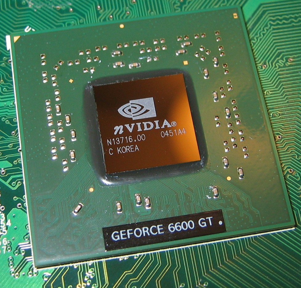
 GeForce 6600 GT AGP
SLI
The Scalable Link Interface (SLI) allows two GeForce 6 cards of the same type to be connected in tandem. The driver software balances the workload to the chips. SLI-capability is limited to select members of the GeForce 6 family; 6500 and above. SLI is only available when using the PCI-Express bus.
Nvidia PureVideo Technology
Nvidia PureVideo technology is the combination of a dedicated video processing core and software which decodes H.264, VC-1, WMV, and MPEG-2 videos with reduced CPU utilization.
Shader Model 3.0
While ATI was the first to deliver Shader Model 2.0 capability to the retail market, Nvidia was the first to deliver Shader Model 3.0 (SM3) capability. SM3 extends SM2 in a number of ways: standard FP32 (32-bit floating-point) precision, dynamic branching, increased efficiency and longer shader lengths are the main additions. Shader Model 3.0 was quickly adopted by game developers because it was quite simple to convert existing shaders coded with SM 2.0/2.0A/2.0B to version 3.0, and it offered noticeable performance improvements across the entire GeForce 6 line.
Caveats
PureVideo functionality varies by model, with some models lacking WMV9 and/or H.264 acceleration.[1]
In addition, motherboards with some VIA and SIS chipsets and an AMD Athlon XP processor seemingly have compatibility problems with the GeForce 6600 and 6800 GPUs. Problems that have been known to arise are freezing, artifacts, reboots, and other issues that make gaming and use of 3D applications almost impossible. These problems seem to happen only on Direct3D based applications and do not affect OpenGL.[citation needed]
Geforce 6 Series comparison
 NVIDIA NV40 GPU
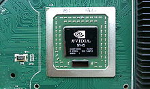 NVIDIA NV45 GPU
Here is how the released versions of the "GeForce 6" series family compare to Nvidia's previous flagship GPU, the GeForce FX 5950 Ultra, in addition to the comparable units of ATI's newly released for the time Radeon X800 and X850 Series:
GeForce FX 5950 Ultra GeForce 6200 TC-32 GeForce 6600 GT GeForce 6800 Ultra ATI Radeon X800 XT PE ATI Radeon X850 XT PE Transistor count 135 million 77 million 146 million 222 million 160 million 160 million Manufacturing process 0.13 µm 0.11 µm 0.11 µm 0.13 µm 0.13 µm low-k 0.13 µm low-k Die Area (mm²) ~200 110 156 288 288 297 Core clock speed (MHz) 475 350 500 400 520 540 Number of pixel shader processors 4 4 8 16 16 16 Number of pixel pipes 4 4 8 16 16 16 Number of texturing units 8(16*) 4 8 16 16 16 Number of vertex pipelines 3* 3 3 6 6 6 Peak pixel fill rate (theoretical) 1.9 Gigapixel/s 700 Megapixel/s 2.0 Gigapixel/s 6.4 Gigapixel/s 8.32 Gigapixel/s 8.64 Gigapixel/s Peak texture fill rate (theoretical) 3.8 Gigatexel/s 1.4 Gigatexel/s 4.0 Gigatexel/s 6.4 Gigatexel/s 8.32 Gigatexel/s 8.64 Gigatexel/s Memory interface 256-bit 64-bit 128-bit 256-bit 256-bit 256-bit Memory clock speed 950 MHz DDR 700 MHz DDR2 1.0 GHz GDDR3 1.1 GHz GDDR3 1.12 GHz GDDR3 1.18 GHz GDDR3 Peak memory bandwidth (GB/s) 30.4 5.6 16.0 35.2 35.84 37.76 (*) GeForce FX series has an Array based Vertex Shader.
GeForce 6800 Series
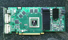 GeForce 6800 Ultra PCI-E 512MB GDDR3
The first family in the GeForce 6 product-line, the 6800 series catered to the high-performance gaming market. As the very first GeForce 6 model, the 16 pixel pipeline GeForce 6800 Ultra (NV40) was 2 to 2.5 times faster than Nvidia's previous top-line product (the GeForce FX 5950 Ultra), packed four times the number of pixel pipelines, twice the number of texture units and added a much improved pixel-shader architecture. Yet, the 6800 Ultra was fabricated on the same (IBM) 130 nanometer process node as the FX 5950, and it consumed slightly less power.
Early benchmarks put the 6800 series at a disadvantage when compared to similarly priced ATI cards. Newer drivers have improved performance on both companies' products. Against the ATI's Radeon X800XT PE, its direct competitor, the 6800 Ultra performed comparably in most synthetic and game benchmarks, with each card showing its individual strengths in different gaming applications. Nvidia's part is strong in many applications programmed for OpenGL (a traditional strength of Nvidia), while ATI leads in many Direct3D applications. Thus, it is now generally accepted that the GeForce 6800 Ultra is similar in performance to the Radeon X800 XT, and that the GeForce 6800 GT generally performs better than the Radeon X800 Pro.
Like all of Nvidia's GPUs up until 2004, initial 6800 members were designed for the AGP bus. Nvidia added support for the PCI Express (PCIe) bus in later GeForce 6 products, usually by use of an AGP-PCIe bridge chip. In the case of the 6800 GT and 6800 Ultra, Nvidia developed a variant of the NV40 chip called the NV45. The NV45 shares the same die core as the NV40, but embeds an AGP-PCIe bridge on the chip's package. (Internally, the NV45 is an AGP NV40 with added bus-translation logic, to permit interfacing with a PCIe motherboard. Externally, the NV45 is a single chip with two separate silicon dies clearly visible on the top.) NV48 is NV45 with 512MB RAM.
The use of an AGP-PCIe bridge chip initially led to fears that natively-AGP GPUs would not be able to take advantage of the additional bandwidth offered by PCIe and would therefore be at a disadvantage relative to native PCIe chips.[citation needed] However, benchmarking reveals that even AGP 4x is fast enough that most contemporary games do not improve significantly in performance when switched to AGP 8x, rendering the further bandwidth increase provided by PCIe largely superfluous.[citation needed] Additionally, Nvidia's on-board implementations of AGP are clocked at AGP 12x or 16x, providing bandwidth comparable to PCIe for the rare situations when this bandwidth is actually necessary.[citation needed]
The use of a bridge chip allowed Nvidia to release a full complement of PCIe graphics cards without having to redesign them for the PCIe interface. Later, when Nvidia's GPUs were designed to use PCIe natively, the bidirectional bridge chip allowed them to be used in AGP cards. ATI, initially a critic of the bridge chip, eventually designed a similar mechanism for their own cards.[citation needed]
Nvidia's professional Quadro line contains members drawn from the 6800 series: Quadro FX 4000 (AGP) and the Quadro FX 3400, 4400 and 4400g (both PCI Express). The 6800 series was also incorporated into laptops with the GeForce Go 6800 and Go 6800 Ultra GPUs.
As of August 2010, NVIDIA and Adobe Flash 10.1 does not provide GPU acceleration for GeForce 6 series as a result HD Video playback through Adobe Flash may suffer from digital artifacts, or extreme video lag on Pentium 4 2.8 GHz or slower systems.[2]
PureVideo and the AGP GeForce 6800
PureVideo expanded the level of multimedia-video support from decoding of MPEG-2 video to decoding of more advanced codecs (MPEG-4, WMV9), enhanced post-processing (advanced de-interlacing), and limited acceleration for encoding. But perhaps ironically, the first GeForce product(s) to offer PureVideo, the AGP GeForce 6800/GT/Ultra, failed to support all of PureVideo's advertised features.
Media player software (WMP9) with support for WMV-acceleration did not become available until several months after the 6800's introduction. User and web reports showed little if any difference between PureVideo enabled GeForces and non-Purevideo cards. The prolonged public silence of Nvidia, after promising updated drivers, and test benchmarks gathered by users led the user community to conclude that the WMV9 decoder component of the AGP 6800's PureVideo unit is either non-functional or intentionally disabled.[citation needed]
In late 2005, an update to Nvidia's website finally confirmed what had long been suspected by the user community: WMV-acceleration is not available on the AGP 6800. Of course, today's standard computers are fast enough to play WMV9 video and other sophisticated codecs like MPEG-4, H.264 or Theora without hardware acceleration.[citation needed]
GeForce 6 series general features
 GeForce 6800 Personal Cinema
- 4, 8, 12, or 16 pixel-pipeline GPU architecture
- Up to 8x more shading performance compared to the previous generation
- CineFX 3.0 engine - DirectX 9 Shader Model 3.0 support
- On Chip Video processor (PureVideo)
- Full MPEG-2 encoding and decoding at GPU level (PureVideo)
- Advanced Adaptive De-Interlacing (PureVideo)
- DDR and GDDR-3 memory on a 256-bit wide Memory interface
- UltraShadow II technology - 3x to 4x faster than NV35 (GeForce FX 5900)
- High Precision Dynamic Range (HPDR) technology
- 128-bit studio precision through the entire pipeline - Floating-point 32-bit color precision
- IntelliSample 4.0 Technology - 16x Anisotropic Filtering, Rotating Grid Antialiasing and Transparency Antialiasing (see here)
- Max Resolution is 2048x1536@85 Hz
- Video Scaling and Filtering - HQ filtering techniques up to HDTV resolutions
- Integrated TV Encoder - TV-output up to 1024x768 resolutions
- OpenGL 2.0 Optimizations and support
- DVC 3.0 (Digital Vibrance Control)
- Dual 400 MHz RAMDACs which support QXGA displays up to 2048x1536 @ 85 Hz
- Dual DVI on select members (Depending on the Card Manufacturer.)
6800 chipset table
Memory Clock Speed: 400 MHz (800 MHz effective) Memory Interface: 128-bits Memory Bandwidth: 12.8 GB/s Fill Rate: 3.2 billion pixel/s and 4.8 billion texel/s Vertex/s: 500 million SLI support (Only for the PCIe version) Cooling Solution: Passively cooled (Nvidia reference) Memory Type: GDDR3 or DDR2 Fabrication process: 90-nm
Board Name Core Type Core
(MHz)Memory
(MHz)Pipeline
ConfigVertex
ProcessorsMemory
Interface6800 Ultra NV40/NV45/NV48 400 1100 16 6 256-bit 6800 GT NV40/NV45/NV48 350 1000 16 6 256-bit 6800 GS NV40/NV42 350/425 1000 12 5 256-bit 6800 GTO NV40/NV45 350 900 12 5 256-bit 6800 NV40/NV41
NV42325 700/600 12 5 256-bit 6800 Go NV41M 300 600 12 5 256-bit 6800 Go Ultra NV41M(0.13u)/NV42M(0.11u) 450 1100 12 5 256-bit 6800 XT NV40/NV41/NV42 325/350/? 700/1000+ 8 4 128/256-bit 6800 XE NV40 275/300/325 533/700 8 3 128-bit 6800 LE NV40 300 700 8 4 256-bit Notes
- The GeForce 6800 GS is cheaper to manufacture and has a lower MSRP than the GeForce 6800 GT because it has fewer pipelines and a smaller process (110 vs 130 nm), but performance is similar because it has a faster core clock. The AGP version, however, uses the original NV40 chip and 6800 GT circuit board and may be capable of re-activating the inactive pixel and vertex pipes. Unfortunately, the PCI Express version lacks them entirely, precluding such modifications.
- The 6800 GTO (which was produced only as an OEM card) contains four masked pixel pipelines and one masked vertex shader, which are potentially unlockable.
- The GeForce 6800 is often unofficially called the "GeForce 6800 Vanilla" or the "GeForce 6800 NU" (for Non-Ultra) to distinguish it from the other models. Recent PCIe variants have the NV41 (IBM 0.13 micrometre) or NV42 (TSMC 0.11 micrometre) cores, which are native PCIe implementations and do not have an integrated AGP bridge chip. The AGP version of the video card contains four masked pixel pipelines and one masked vertex shader, which are potentially unlockable through software mods. PCI-Express 6800 cards are incapable of such modifications, because the extra pixel pipelines and vertex buffers are nonexistent.
- The 6800 XT varies greatly depending on manufacturer. It is produced on three cores (NV40/NV41/NV42), four memory configurations (128 MB DDR, 256 MB DDR, 128 MB GDDR3, 256 MB GDDR3, and 512 MB GDDR2), and has clock speeds ranging from 300-425 (core) and 600-1000 (memory). 6800 XT cards based on the NV40 core contain eight masked pixel pipelines and two masked vertex shaders, and those based on the NV42 core contain four masked pipelines and one masked shader (for some reason, the NV42 cards are almost never unlockable. It is speculated that the pipelines are being laser-cut).
- The 6800 LE contains eight masked pixel pipelines and two masked vertex shaders, which are potentially unlockable.
- The AGP version of the 6800 series does not have support for 2D acceleration in Adobe Reader/Acrobat 9.0 even though the GeForce AGP 6600, and PCI-E 6800 versions do.[3]
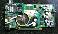
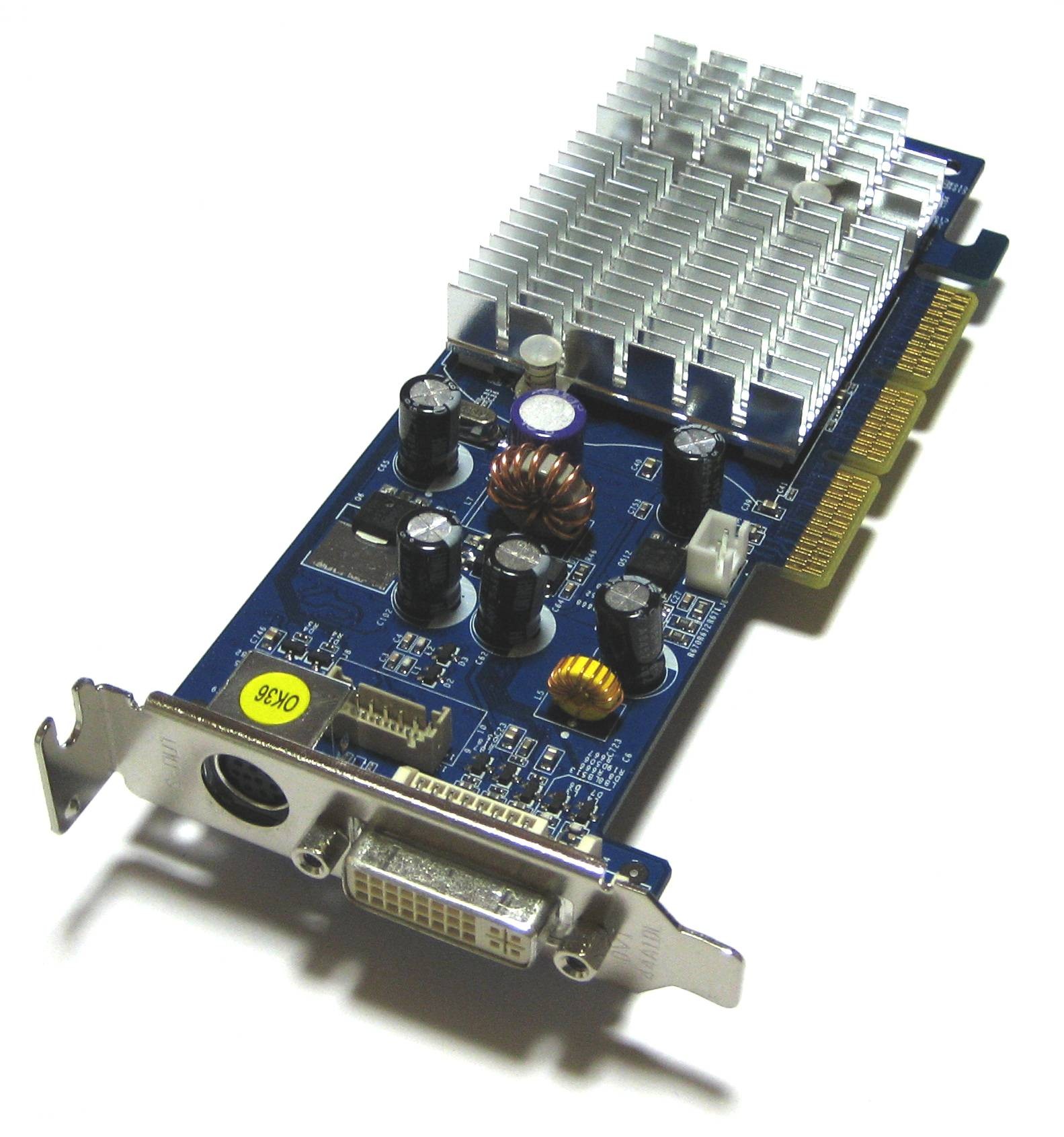
GeForce 6600 Series
 GeForce 6600 GT Personal Cinema
The GeForce 6600 (NV43) was officially launched on August 12, 2004, several months after the launch of the 6800 Ultra. With half the pixel pipelines and vertex shaders of the 6800 GT, and a smaller 128-bit memory bus, the lower-performance and lower-cost 6600 is the mainstream product of the GeForce 6 series. The 6600 series retains the core rendering features of the 6800 series, including SLI. Equipped with fewer rendering units, the 6600 series processes pixel data at a slower rate than the more powerful 6800 series. However, the reduction in hardware resources, and migration to TSMC's 110 nm manufacturing process (versus the 6800's 130 nm process), make the 6600 both less expensive for Nvidia to manufacture and less expensive for customers to purchase.
Their 6600 series currently has three variants: the GeForce 6600LE, the 6600, and the 6600GT (in order from slowest to fastest.) The 6600 GT performs quite a bit better than the GeForce FX 5950 Ultra or Radeon 9800 XT, with the 6600 GT scoring around 8000 in 3DMark03, while the GeForce FX 5950 Ultra scored around 6000, and it is also much cheaper. Notably, the 6600 GT offered identical performance to ATI's high-end X800 PRO graphics card with drivers previous December 2004, when running the popular game Doom 3 (afterwards ATI optimized their drivers and was able to distance itself slightly from the 6600GT). It was also about as fast as the higher-end GeForce 6800 when running games without anti-aliasing in most scenarios.
At introduction, the 6600 family was only available in PCI Express form. AGP models became available roughly a month later, through the use of Nvidia's AGP-PCIe bridge chip. A majority of the AGP GeForce 6600GTs have their memory clocked at 900 MHz, which is 100 MHz below the PCI-E card, on which the memory operates at 1000 MHz. This can contribute to a performance decline when playing certain games. However, many times it is possible to "overclock" the memory to its nominal frequency of 1000 MHz.
6600 chipset table
Board Name Core Type Core
(MHz)Memory
(MHz)Pipeline
ConfigVertex
ProcessorsMemory
Interface6700 XL NV43 525 1100 8 3 128-bit 6600 GT GDDR3 NV43 500 900/1000 8 3 128-bit 6600 XL NV43 400 800 8 3 128-bit 6600 DDR2 NV43 350 800 8 3 128-bit 6600 NV43 300 500/550 8 3 128-bit 6600 LE NV43 300 500 4 3 128-bit  NVIDIA NV43 GPU
Other data for PCI Express based cards:
- Memory Interface: 128-bit
- Memory Bandwidth: 16.0 GB/s.
- Fill Rate (pixels/s.): 4.0 billion
- Vertices per Second: 375 million
- Memory Data Rate: 1000 MHz
- Pixels per Clock (peak): 8
- RAMDACs: 400 MHz
Other data for AGP based cards:
- Memory Interface: 128-bit
- Memory Bandwidth: 14.4 GB/s.
- Fill Rate (pixels/s.): 4.0 billion
- Vertices per Second: 375 million
- Memory Data Rate: 900 MHz
- Pixels per Clock (peak): 8
- RAMDACs 400 MHz
GeForce 6500
The GeForce 6500 was released in October 2005 and is based on the same NV44 core as the value/budget (low-end or entry level) GeForce 6200TC, but with a higher GPU clock speed and more memory. The GeForce 6500 also supports SLI.
GeForce 6500
- Core Clock: 450 MHz
- Memory Clock: 700 MHz
- Pixel Pipelines: 4
- Number of ROPs: 2
- Vertex Processors: 3
- Memory: 128 MB/256 MB DDR on a 64-bit interface
- Fill Rate (pixels/s): 1.6 billion
- Vertices per Second: 300 million
- Effective Memory Bandwidth(GB/s): 13.44
GeForce 6200
 GeForce 6200 in a low-profile AGP form factor
With just 4 pixel pipelines, the 6200 series forms Nvidia's value/budget (low-end or entry level) product. The 6200 omits memory compression and SLI support, but otherwise offers similar rendering features as the 6600s. The later 6200 boards were based on the NV44 core (s), which is the final production silicon for the 6200 series.
However, at introduction, production silicon was not yet ready. Nvidia fulfilled 6200 orders by shipping binned/rejected 6600 series cores (NV43V). The rejects were factory modified to disable four-pixel pipelines, thereby converting the native 6600 product into a 6200 product. Some users were able to "unlock" early 6200 boards through a software utility (effectively converting the 6200 back into a 6600 with the complete set of eight pixel pipelines total) if they owned boards with an NV43 A2 or earlier revision of the core. Thus, not all NV43-based 6200 boards could successfully be unlocked (specifically, those with a core revision of A4 or higher), and as soon as NV44 production silicon became available, Nvidia discontinued shipments of downgraded NV43V cores.
GeForce 6200 chip specifications
GeForce 6200
- Core Clock: 300 MHz
- Memory Clock: 550 MHz
- Pixel Pipelines: 4
- Vertex Processors: 3
- Memory: 128 MB/256 MB/512 MB [4] DDR on a 64-bit/128-bit interface
GeForce 6200 TurboCache / AGP
The GeForce 6200 TurboCache / AGP (NV44/NV44a) is a natively four-pipeline version of the NV43. GeForce 6200 TurboCache cards only have a very small (by modern standards) amount of memory, but make up for this by using system memory accessed through the PCI-Express bus.
GeForce 6200 TurboCache / AGP chip specifications
GeForce 6200 PCI-Express (NV44) TurboCache
- Core Clock: 350 MHz
- Memory Clock: 700 MHz
- Pixel Pipelines: 4
- Number of ROPs: 2
- Vertex Processors: 3
- Memory: 16 MB/32 Mb/64 Mb/128 Mb DDR on a 32-bit/64-bit/128-bit interface
- GeForce 6200 w/ TurboCache supporting 128 MiB, including 16 Mb of local TurboCache (32-bit)
- GeForce 6200 w/ TurboCache supporting 128 MiB, including 32 Mb of local TurboCache (64-bit)
- GeForce 6200 w/ TurboCache supporting 256 MiB, including 64 Mb of local TurboCache (64-bit)
- GeForce 6200 w/ TurboCache supporting 256 MiB, including 128 Mb of local TurboCache (128-bit)
GeForce 6200 AGP (NV44a) without TurboCache
- Core Clock: 350 MHz
- Memory Clock: 500 MHz
- Pixel Pipelines: 4
- Number of ROPs: 2
- Vertex Processors: 3
- Memory: 128-256-512 MB DDR or DDR2 on a 64-bit interface
GeForce 6200 AGP (NV44a2) without TurboCache
- Core Clock: 350 MHz
- Memory Clock: 540 MHz
- Pixel Pipelines: 4
- Number of ROPs: 2
- Vertex Processors: 3
- Memory: 128 MB DDR2 with a 128-bit interface
- Cooling: Passive heatsink
(Only PNY is known to manufacture this card, which appears to be discontinued.)
GeForce 6200 PCI (NV44) without TurboCache
BFG Technologies originally introduced a unique PCI variant of the GeForce 6200 via its namesake B.F.G. and 3D Fuzion product lines. Subsequently PNY (GeForce 6200 256 MB PCI), SPARKLE Computer (GeForce 6200 128 MB PCI and GeForce 6200 256 MB PCI), and eVGA (e-GeForce 6200 256 MB PCI) released their own PCI versions of the Geforce 6200 featuring higher memory clocks and resultant memory bandwidth.
Until the release of the ATI X1300 PCI, these were the only PCI DirectX 9 capable cards not based on previous generation GeForce5 FX technology or discontinued XGI Technology Volari V3XT chipsets.
Excluding SPARKLE's GeForce 8400 and 8500 series cards, currently[as of?] the enhanced 256 MB Geforce 6200 PCI [5] variants remain the most powerful PCI based solutions available; making these cards desired by users lacking the option of upgrading to an AGP or PCI Express based discrete video card.
- Core Clock: 350 MHz
- Memory Clock: 400 MHz (BFG Technologies 6200 oc 410 MHz, PNY and EVGA 533 MHz)
- Pixel Pipelines: 4
- Memory: 256 (BFG Technologies 6200 OC PCI and EVGA e-Ge-Force 6200 PCI) / 128 (BFG Technologies 3DFuzion GeForce 6200 PCI) MB DDR on a 64-bit interface
GeForce 6100 and 6150 series
In late 2005 Nvidia introduced a new member to the GeForce family, the 6100 series, also known as C51. The term GeForce 6100/6150 actually refers to an nForce4-based motherboard with an integrated NV44 core, as opposed to a standalone graphics card. Nvidia released this product both to follow up its immensely popular GeForce4 MX based nForce and nForce2 boards and to compete with ATI's RS480/482 and Intel's GMA 900/950 in the integrated graphics space. The 6100 series is very competitive, usually tying with or just edging out the ATI products in most benchmarks.
The motherboards use two different types of southbridges - the nForce 410 and the nForce 430. They are fairly similar in features to the nForce4 Ultra motherboards that were on the market before them. Both feature PCI Express and PCI support, eight USB 2.0 ports, integrated sound, two Parallel ATA ports, and Serial ATA 3.0 Gbit/s with Native Command Queuing (NCQ) – two SATA ports in the case of the 410, four in the 430. The 430 southbridge also supports Gigabit Ethernet with Nvidia's ActiveArmor hardware firewall, while the 410 supports standard 10/100 Ethernet only.
GeForce 6100 and 6150 series chip specifications
Both the 6100 and 6150 support Shader Model 3.0 and DirectX 9.0c. The 6150 also features support for High-Definition video playback, PureVideo Processing, DVI, and video-out while the 6100 supports PureVideo Processing only. Maximum supported resolution is 1920 x 1440 pixels (@75 Hz) for RGB display and 1600 x 1200 pixels (@65 Hz) for DVI-D display
GeForce 61XX abnormally high failure rate in notebook computers
In 2008, Nvidia took a $150 to 250M charge against revenue because the GPUs were failing at "higher than normal rates."[6] HP provided an extension to their warranty of up to 24 months for notebooks affected by this issue. A class action suit was filed against HP and Nvidia by Whatley Drake & Kallas LLC.
GeForce 6100
- Manufacturing process: 90 nm
- Core Clock: 425 MHz
- Vertex Processors: 1
- Pixel Pipelines: 2
- Shader Model: 3
- DirectX support: v9.0c
- Video playback acceleration: SD video acceleration (HD video acceleration not supported)
- Outputs: VGA only
- Memory: Shared DDR/DDR2 (socket 939/AM2) system memory (selectable through BIOS - usually 32/64/128/256 MB)
GeForce 6150
- Manufacturing process: 90 nm
- Core clock: 475 MHz[7]
- Vertex processors: 1
- Pixel pipelines: 2
- Shader model: 3
- DirectX support: v9.0c
- Video playback acceleration: HD video acceleration
- Outputs: VGA, DVI, RCA (Video)
- Memory: Shared DDR2 (socket 939/AM2) system memory (selectable through BIOS - usually 32/64/128/256 MB)
- HT Bus (Bandwidth) = 2000 MT/s max
GeForce 6150LE
GeForce 6150LE is used by Fujitsu Siemens in the Esprismo green desktop and the Compaq Presario SR-1915 Desktop. The chip is also used by HP in the HP Pavilion Media Center a1547c Desktop PC and by Dell in the C521 Desktop PC.
GeForce 6150SE
GeForce 6150SE (MCP61, also known as C61) is an updated, single-chip version of the Nvidia GeForce 6100. The MCP61 uses less power than the original C51 2-chip version of 6100. Its onboard video outperforms the 6150 in many 3D benchmarks despite its lower core frequency (425 MHz), because of added hardware Z-culling.
MCP61 introduced a bug in the SATA NCQ implementation. As a result, Nvidia employees have contributed code to disable NCQ operations under Linux.[8]
- Manufacturing process: 90 nm
- Core Clock: 425 MHz
- HT Bus = 2000 max
- Vertex Processors: 1
- Pixel Pipelines: 2
- Shader Model: 3
- DirectX support: v9
Outputs: VGA only
IntelliSample 4.0 and the GeForce 6 GPUs
Upon launch of the GeForce 7 family of graphics processing units, IntelliSample 4.0 was considered to be an exclusive feature of the GeForce 7 series of GPUs. However, version 91.47 (and subsequent versions) of the Nvidia ForceWare drivers enable the features of IntelliSample 4.0 on the GeForce 6 GPUs. IntelliSample 4.0 introduces two new antialiasing modes, known as Transparency Supersampling Antialiasing and Transparency Multisampling Antialiasing. These new antialiasing modes enhance the image quality of thin-lined objects such as fences, trees, vegetation and grass in various games.
One possible reason for the enabling of IntelliSample 4.0 for GeForce 6 GPUs might be the fact that the GeForce 7100 GS GPUs are based on NV44 chips, the same as the GeForce 6200 models. Because of this, Nvidia had to backport IntelliSample 4.0 features to the NV4x GPUs, and as a result, the entire GeForce 6 family is able to enjoy the benefits of Transparency Antialiasing.
It was already well known across various communities that Transparency Antialiasing could be used on GeForce 6 GPUs by using some third party tweak tools. As of Nvidia ForceWare drivers 175.16, GeForce 6 IntelliSample 4.0 support has been removed.
See also
- Comparison of Nvidia graphics processing units
- Graphics hardware and FOSS
- GeForce FX Series
- GeForce 7 Series
- Scalable Link Interface
Notes and references
- ^ Nvidia PureVideo - Product Comparison
- ^ NVIDIA Flash 10.1 Hardware Support List
- ^ Adobe Knowledge Base - 2D Graphics Acceleration (GPU) support in Acrobat and Adobe Reader (9.0 on Windows)
- ^ Newegg.com - CHAINTECH SA62A-512 GeForce 6200 512 MB 64-bit DDR2 SDRAM AGP 4X/8X Video Card - Retail
- ^ BFG NVIDIA GeForce 6200 OC 256MB PCI.
- ^ http://www.nvidia.com/object/io_1215037160521.html
- ^ Tech Specs
- ^ http://www.spinics.net/lists/linux-ide/msg15779.html
External links
- Nvidia: GeForce 6 Series Product Overview
- Nvidia PureVideo Technology page
- Inside nVidia NV40
- Transparency Antialiasing on GeForce 6 GPUs
- Nvidia: Integrated GPU Technical Specifications
Reviews
- nvNews/ a nvnews review of the GeForce 6800
- Beyond 3D/ preview of nv45 core architecture
- Guru3D Nvidia GeForce 6 Series and ATi X Series/comparison - 6-series v. Radeon X-series
- X-bit Labs Second Generation of Integrated Graphics from Nvidia: GeForce 6150 and GeForce 6100/ Page on GeForce 6100, 6150
- GeForce 6600GT review/ review- GeForce 6600GT
- nVidia Performance webpage for GeForce FX 5700 and higher models with detailed specifications of GeForce FX 5950 Ultra/Nvidia page on GeForce FX-series.
Nvidia Graphics processing units Early chipsetsRIVA seriesGeForce 256 · GeForce 2 · GeForce 3 · GeForce 4 · GeForce 5 · GeForce 6 · GeForce 7 · GeForce 8 · GeForce 9 · GeForce 100 · GeForce 200 · GeForce 300 · GeForce 400 · GeForce 500Other seriesTechnologiesMotherboard chipsets GeForce SeriesnForce SeriesnForce 220/415/420 · nForce2 · nForce3 · nForce4 · nForce 500 · nForce 600 · nForce 700 · nForce 900TechnologiesOther products Project DenverBridge chipsHandheldSoftwareAcquisitionsKey people Jen-Hsun Huang · Chris Malachowsky · Curtis Priem · David Kirk · Debora Shoquist · Dr. Ranga Jayaraman · Jonah M. AlbenCategories:- 2004 introductions
- Nvidia
- Video cards


Wikimedia Foundation. 2010.