- Semiconductor process simulation
Semiconductor process simulation is the modeling of the fabrication of semiconductor devices such as
transistor s. It is a branch ofelectronic design automation , and part of a sub-field known astechnology CAD , or TCAD.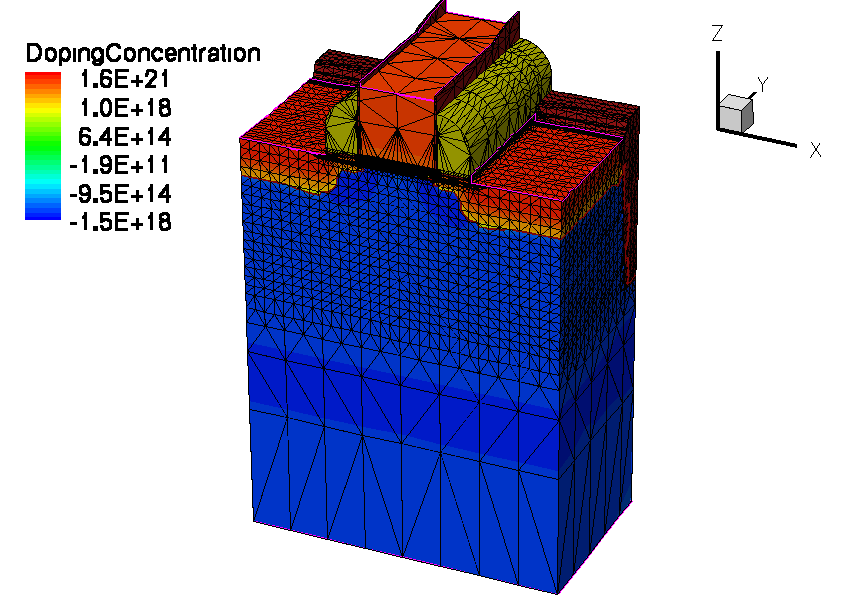
400px|right|thumb|This figure shows a result from semiconductor process. The input is a description of the semiconductor fabrication process; the result as shown here is the final geometry and the concentrations of all the dopants. This will then be used by other programs to predict the electrical properties of the devices formed. (CRC Electronic Design Automation for IC Handbook, Chapter 24)The ultimate goal of process simulation is an accurate prediction of the active
dopant distribution, the stress distribution and the device geometry. Process simulation is typically used as an input for device simulation, the modeling of device electrical characteristics. Collectively process and device simulation form the core tools for the design phase known as TCAD or Technology Computer Aided Design. Considering theintegrated circuit design process as a series of steps with decreasing levels of abstraction,logic synthesis would be at the highest level and TCAD, being closest to fabrication, would be the phase with the least amount of abstraction. Because of the detailed physical modeling involved, process simulation is almost exclusively used to aid in the development of single devices whether discrete or as a part of anintegrated circuit .The fabrication of integrated circuit devices requires a series of processing steps called a process flow. Process simulation involves modeling all essential steps in the process flow in order to obtain dopant and stress profiles and, to a lesser extent, device geometry. The input for process simulation is the process flow and a layout. The layout is selected as a linear cut in a full layout for a 2D simulation or a rectangular cut from the layout for a 3D simulation.
TCAD has traditionally focused mainly on the transistor fabrication part of the process flow ending with the formation of source and drain contacts -- also known as front end of line manufacturing. Back end of line manufacturing, e.g. interconnect and dielectric layers are not considered. One reason for delineation is the availability of powerful analysis tools such as electron microscopy techniques, scanning electron microscopy (SEM) and
transmission electron microscopy (TEM), which allow for accurate measurement of device geometry. There are no similar tools available for accurate high resolution measurement of dopant or stress profiles. Nevertheless, there is growing interest to investigate the interaction between front end and back end manufacturing steps. For example, back end manufacturing may cause stress in the transistor region changing device performance. These interactions will stimulate the need for better interfaces to back end simulation tools or lead to integration of some of those capabilities into TCAD tools.In addition to the recent expanding scope of process simulation, there has always been a desire to have more accurate simulations. However, simplified physical models have been most commonly used in order to minimize computation time. But, shrinking device dimensions put increasing demands on the accuracy of dopant and stress profiles so new process models are added for each generation of devices to match new accuracy demands. Many of the models were conceived by researchers long before they were needed, but sometimes new effects are only recognized and understood once process engineers discover a problem and experiments are performed. In any case, the trend of adding more physical models and considering more detailed physical effects will continue and may accelerate.
History
The history of commercial process simulators began with the development of the Stanford University Process Modeling (SUPREM) program . Building upon this beginning with improved models SUPREM II and SUPREM III were developed. Technology Modeling Associates, Inc. (TMA) which was formed in 1979 was the first company to commercialize SUPREM III. Later Silvaco also commercialized SUPREM and named the product ATHENA. TMA commercialized SUPREM-IV (2D version) and called it TSUPREM4. In 1992, Integrated Systems Engineering (ISE) came out with the 1D process simulator TESIM and the 2D process simulator DIOS. At about the same time development of a new 3D process and device simulator began at TMA and after TMA was acquired by Avanti, the product was released in 1998 as Taurus. Around 1994 a first version of the Florida Object Oriented Process Simulator (FLOOPS) was completed. FLOOPS was later commercialized by ISE in 2002. One other process simulator PROPHET was created around 1994 at Bell labs which later became Agere, but has not been sold commercially. In 2002
Synopsys acquired Avant!, corp. and in 2004 Synopsys acquired ISE. Synopsys has announced that a new process simulator will be released in mid 2005 combining the best features of Taurus, TSUPREM4, into the FLOOPS platform and will be called Sentaurus Process. Besides these simulators, there are numerous other university and commercial simulators such as PROMIS, PREDICT, PROSIM, ICECREAM, DADOS, TITAN, MicroTec, DOPDEES, ALAMODE.Process simulation methods
The process steps most often associated with process simulation are
ion implantation , annealing (diffusion and dopant activation), etch, deposition, oxidation, andepitaxy . Other common steps includechemical-mechanical planarization (CMP), silicidation, and reflow.All commercial process simulators use a combination of the
finite element analysis (FE) and/orfinite volume method s (FV) methods. A complete description of FE/FV method is out of the scope of this article but there are many fine books which describe the topic thoroughly. However, it is important to discuss requirements for process simulation for achieving accurate results. These requirements are based on the same requirements as generic to FE/FV techniques with an additional difficulty coming from the changes in the geometry during the simulated fabrication of the device. Process simulation uses an FE/FV mesh to compute and store the dopant and stress profiles. Each geometrical change in the simulation domain requires a new mesh which fits to the new boundaries. As will be described below, the large number of geometry modifying steps involved and the nature of process simulation where each step depends on the cumulative results of all previous steps, make process simulation an especially challenging application of the FE/FV technique.One of the most important results of process simulation is the dopant profile after processesing. The accuracy of the profile strongly depends on maintaining a proper density of mesh points at any time during the simulation. The density of points should be just enough to resolve all dopant and defect profiles but not more because the computation expense of solving the diffusion equations increases with the number of mesh points. A typical full flow CMOS process simulation can have more than 50 mesh changes and the number of mesh changes can increase dramatically if adaptive meshing is performed. For each mesh change, interpolation is used to obtain data values on the new mesh. It is important to manage the mesh changes in such a way to avoid accuracy degradation due to interpolation error. The easiest way to do this is to always keep points once they are introduced into the mesh, but this has the drawback of producing very many mesh points which can be computationally expensive. Maintaining a balance between interpolation error, computational expense, and minimization of required user input is important for obtaining accurate results with a minimum of computational expense. This is especially true when simulating devices in 3D. Without careful placement of mesh either the accuracy will suffer unacceptably, or the computational expense will be too great to be useful. Process simulation tools so far have had limited success in completely automating mesh adaptation such that no user intervention is required. This places a requirement of the user to understand meshing and how it affects simulation accuracy and run time and the burdens the user to track mesh changes during the simulation to ensure proper mesh is maintained.
One of the most important uses of TCAD tools is to explore new device technology where many exploratory simulations are performed in order to give the device designer a better understanding of possible benefits as well as drawbacks of a given technology. This use case demands sequential simulations with some analysis in between. In order to be useful, many simulation cycles must be run within the time allotted for exploration, putting a high priority on minimization of simulation run time. Currently, full flow standard CMOS simulations are most often accomplished with a combination of 1D and 2D simulation and take less than a few hours on a 2.6 GHz Pentium 4. To perform these simulations in 3D (from gate formation on) would take a minimum of 24 hours for minimum accuracy simulation. Most of the information desired from TCAD simulations can be extracted from the simplification that the device can be treated uniformly in depth (i.e. a 2D simulation). To include the effects device shape along the depth or to investigate implant shadowing, 3D simulations must be performed.
References
"Electronic Design Automation For Integrated Circuits Handbook", by Lavagno, Martin and Scheffer, ISBN 0-8493-3096-3 A survey of the field of
electronic design automation . This summary was derived (with permission) from Vol II, Chapter 24, "Process Simulation", by Mark Johnson.
Wikimedia Foundation. 2010.