- JESD204
-
JEDEC JESD204A (2008) is a new industry standard for the interconnection of digital-to-analog converter (DAC or D-to-A) or analog-to-digital converter (abbreviated ADC, A/D or A to D) and logic devices which supports the concept of multiple synchronously bonded serial data lanes. The technical details of this new data converter interface standard is the subject of this article.
The advanced feature set enabled by the low overhead JEDEC JESD204A digital interface presents a new design-in option for high-speed data acquisition engineers across the electronics industry. JESD204A is supported by industry standard FPGA families.
Contents
History
- April 2006, JESD204 First revision.
- April 2008, JESD204A Second revision of JESD204
- June 2009, NXP Semiconductors first introduce JESD204A products in the market
JEDEC JESD204A Serialization
In April 2008, the JEDEC Solid State Technology Association JC-16 Committee on Interface Technology published the JESD204A specification, which is a significant revision to the JESD204 specification, published in 2006.
The key enhancement offered by JESD204A is the support beyond single lane links, to multiple time-aligned (synchronized) lanes per link. This enhancement enables the use of much higher bandwidth data converters, as well as multiple synchronized data converter channels. Specifically, the JESD204 specification, with only one lane defined at 3.125 Gbit/s, limits a single-channel 16-bit data converter to a sample rate of

Thus, limits a dual-channel 16-bit data converter to 97.65 MHz.
JESD204A allows a single-channel data converter to multiplex its digital I/O across multiple lanes. For example, a 16-bit single-channel ADC multiplexing its output across four lanes has the potential to support a maximum sampling rate of

The use of a high-speed serial interface brings the additional benefit of IC package I/O pin reduction. For example, using conventional parallel LVDS I/O, a dual-channel 14-bit ADC requires (2 × 14) = 28 interconnect wires. By comparison, JESD204A defines a differential data lane, consuming two interconnect wires, each with
 of maximum raw link bandwidth.
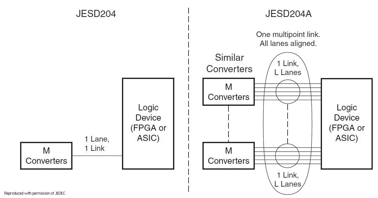
Following typical open systems models, the JESD204A specification includes an electrical PHY layer protocol, a transport layer protocol, and a data link layer protocol, and as noted above, adds an important new capability to the existing JESD204 specification: the ability to support multiple time-aligned lanes in a single data link protocol structure. JESD204A also allows a single ASIC (including DSP and microcontroller) or FPGA to support multiple (or multi-point) links, figure 1.
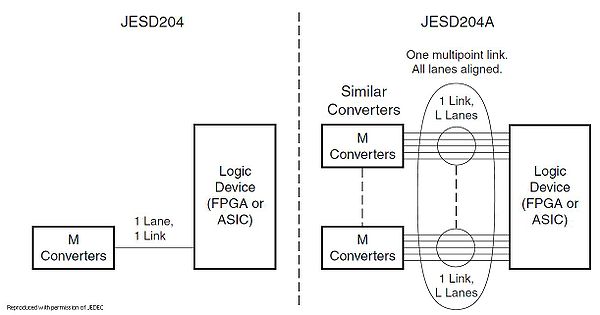 Figure 1 – JESD204 (2006) versus JESD204A (2008)
Note that the scope of JEDEC JESD204A is constrained to the interactions between one logic device (FPGA or ASIC) and one or more converter devices (digital-to-analog converter or analog-to-digital converter). Time-aligned synchronization of two or more ADC channels or DAC channels is a requirement in many data acquisition systems, particularly in modern communications systems. For example, many wireless communications systems such as GSM/GPRS/EDGE cell phone systems rely on quadrature sampling techniques to reduce the minimum Nyquist sampling frequency and thus the bandwidth of the data processed by the downstream digital baseband processor, with the goal of reducing power, PCB area and BOM cost. In multi-carrier communications systems, such as those based on OFDM (including 3GPP Long Term Evolution, IEEE 802.11 and IEEE 802.16) fundamentally rely on quadrature sampling and on the preservation of precise phase information in the transmitter and receiver. OFDM systems must preserve phase coherency at the sample level for the digital signal processing algorithms to be valid. In the past, communication system engineers had to use proprietary synchronization techniques (typically involving shallow FIFOs and state machines) at the board-level to guarantee quadrature sample synchronization. The JEDEC JESD204A specification is intended to address this commonly found technical requirement, and foster interoperability among data converters and commonly used logic devices such as FPGA.
The JESD204A Physical Layer
Note that data converters typically utilize a low pin count control/status bus to configure and monitor the functional characteristics of the JEDEC JESD204A interface; the details of control and status register interfaces are explicitly outside the scope of the JEDEC specification. The JESD204A electrical PHY layer defines a SERDES-based differential serial protocol which is unidirectional and point-to-point, operating with self-clocked 8B/10B coded data at rates from 312.5 Mbit/s to 3.125 Gbit/s. Transmitter devices (ADCs, FPGAs, or ASICs) and receiver devices (DACs, FPGAs, or ASICs) on the same FR-4 printed circuit board are guaranteed to operate up to 3.125 Gbit/s on copper traces at least 20 cm in length with full signal integrity if the PHY implementation is complaint to the JESD204A specification.
Transmitters and receivers can also be on separate PCBs connected through a backplane with impedance-controlled connectors or through shielded twisted-pair cables with impedance-controller connectors. JESD204A compliant devices are not required to support the full data rate range of 312.5 Mbit/s to 3.125 Gbit/s. Note that the link bandwidth range 312.5 Mbit/s to 3.125 Gbit/s includes the 8B/10B encoding overhead, so the actual payload data transfer rate is lower. 8B/10B encoding has the dual merits of utilizing a computed running disparity to maintain DC balance (zero DC offset) in the electrical signal (allowing the signal to be high-pass optically, capacitively or inductively coupled) and the ability to detect single-bit errors at the receiver.
The running disparity is a continuously computed binary value (interpreted as either + or -) that enables the 8B/10B state machine to select one of two appropriate output bit patterns (called a valid code group in the specification) to maintain long-term DC balance.
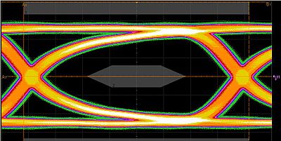
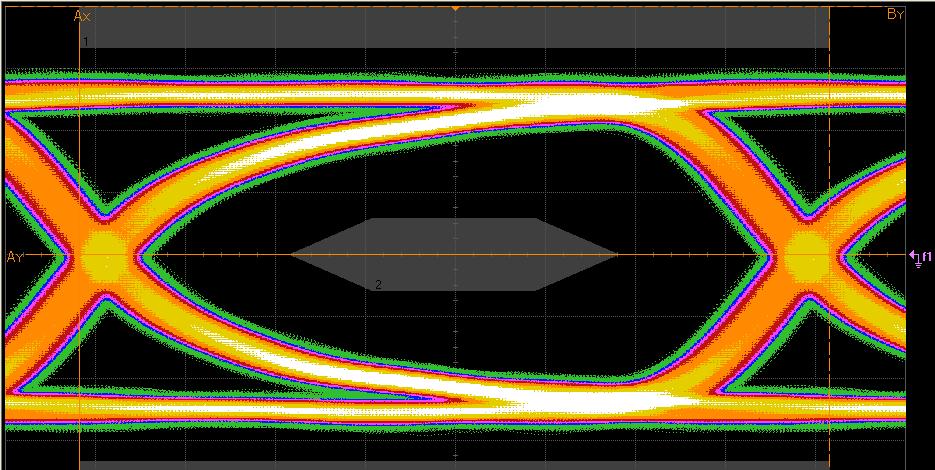
The electrical signaling defined by JESD204A is low-swing/low-voltage and differential. It complies with what is widely known as CML (Current Mode Logic), used in the DVI and HDMI standards for digital audio and video transmission. Consistent with CML, JESD204A specifies 100-ohm transmission line termination at 1.2V. JESD204A compliant transmitters and receivers must achieve a Bit Error Rate (BER) of less than 10-12. Transmitters and receivers may be either fully DC-compliant or AC-compliant only. AC-compliant only devices must be coupled with external capacitors. This standard also defines transmit and receive eye diagram masks and related jitter specifications to which compliant devices must conform.
 The JESD204A standard defines one more flexibility point: the possibility to extend the transmission length up to 40cm. As a matter of fact, NXP’s implementation of this standards exhibits a widely opened eye diagram even over a 1m long transmission PCB trace
JESD204A defines three logical signals per link:
- The first logical signal is the lane, which is the differential 8B/10B self-clocked encoded CML signal.
- The second logical signal is the frame clock, which is the shared clock signal for sequencing control and data frames and maintaining the frame alignment. The low-voltage frame clock is distributed to all transmitter and receiver devices connected to the link (all data converters and the FPGA/ASIC logic device). The frame clock (or a multiple/sub-multiple) is also generally used as the data converter sample clock, the absolute timing reference for the transmitter/receiver system, and must exhibit low jitter (including both random and deterministic jitter contributions). Because of this low jitter requirement, the frame clock should not be derived from the recovered serial data link clock at the receiver. Note that the frame clock may be implemented as a differential pair (LVDS or CML).
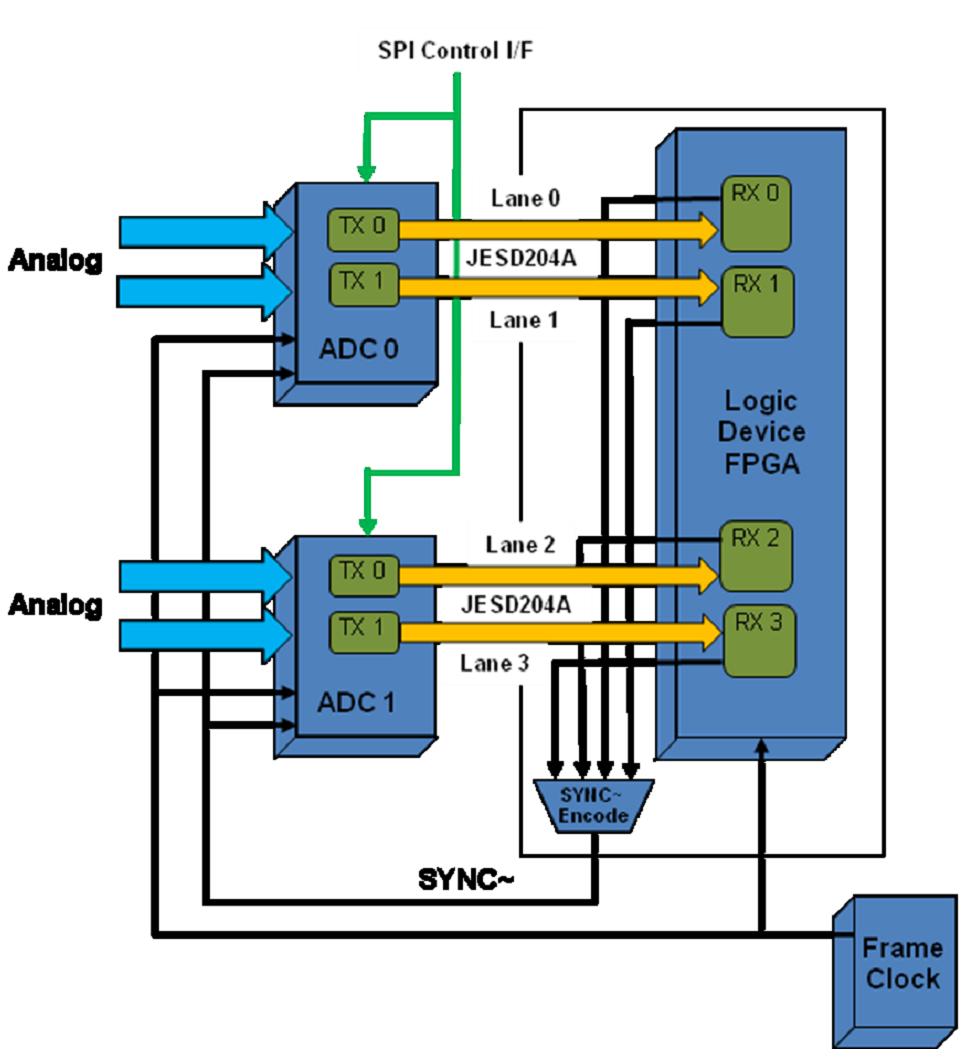
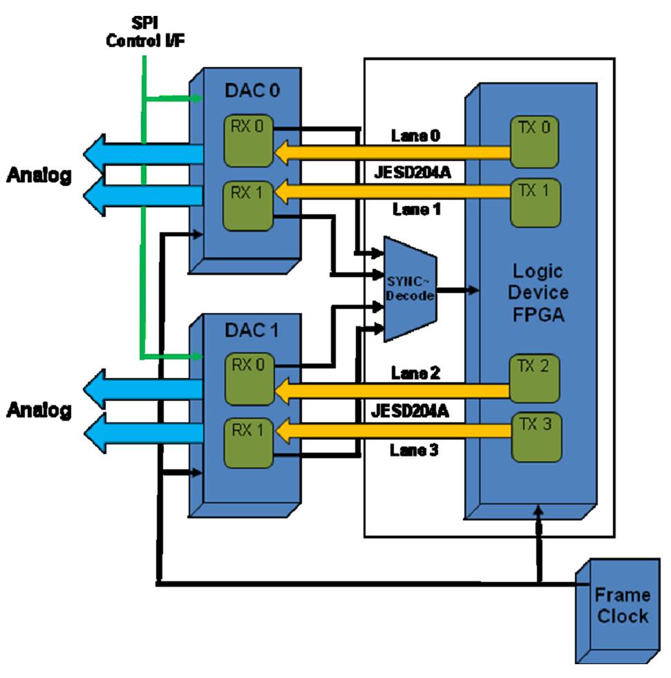
- The third logical signal is the active-low SYNC~, which is a time-critical return path hardware signal from the JESD204A DAC/ASIC receiver (or receivers) to the ADC /ASIC transmitter (or transmitters) that indicates when the link must be initially synchronized, periodically resynchronized or when a data error has occurred. SYNC~ must be synchronous with respect to the frame clock input to the transmitter, and the JEDEC specification includes propagation delay, setup and hold time requirements. Note that SYNC may be implemented as a differential pair (LVDS or CML). In systems with multiple DAC devices (i.e., separate chips), the individual SYNC~ signals must be combined (logically ORed typically) into a single logical subsystem SYNC~, and presented to the FPGA/ASIC transmitter (more on this below). SYNC~ signal skew must be managed by the system designer; the JESD204A specification includes several tables of requirements for skew management. Figure 2 and Figure 3 are illustrations of generic example multi-point ADC and DAC links.
 Figure 2 – ADC Multi-point Link Generic Example
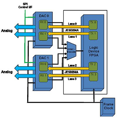 Figure 3 – DAC Multi-point Link Generic Example
It is, in part, by virtue of the fact that there is a single frame clock and a single logical SYNC~ per JESD204A subsystem that sample time-alignment (and thus precise phase coherency) is possible among the data lanes.
Note that the JEDEC JESD204A standard does not address itself to the lane-to-lane synchronization of multiple DAC devices (separate DAC IC packages), which is required for precise analog output phase alignment. The standard assumes the multiple DACs will be similar components from the same data converter manufacturer, so the specification of the inter-device, lane-to-lane synchronization mechanism is left open for innovation, though it is assumed to operate at the frame clock rate, and the user is not expected to have to provide a separate clock.
It is logical to assume that data converter vendors would employ the same lane-to-lane synchronization mechanism used inside single package devices with multiple lanes and multiple DACs, and publish the details necessary for this mechanism to be used at the board level. The JEDEC JESD204A specification assumes this mechanism would not necessarily be inter-operable between DAC vendors. Note that in the JEDEC JESD204A specification, the link connecting a logic device (FPGA, ASIC, processor) with multiple ADCs or DACs is called a “multi point link”. This terminology is potentially confusing (“multi-point” in this usage is not synonymous with multi-drop), as the JESD204A standard defines a point-to-point interconnect (one transmitter is always connected to just one receiver). The specification also defines four device classes:
NMCDA-SL No Multiple Converter Device Alignment – Single Lane NMCDA-ML No Multiple Converter Device Alignment – Multiple Lane MCDA-SL Multiple Converter Device Alignment – Single Lane MCDA-ML Multiple Converter Device Alignment – Multiple Lane The JESD204A Transport Layer
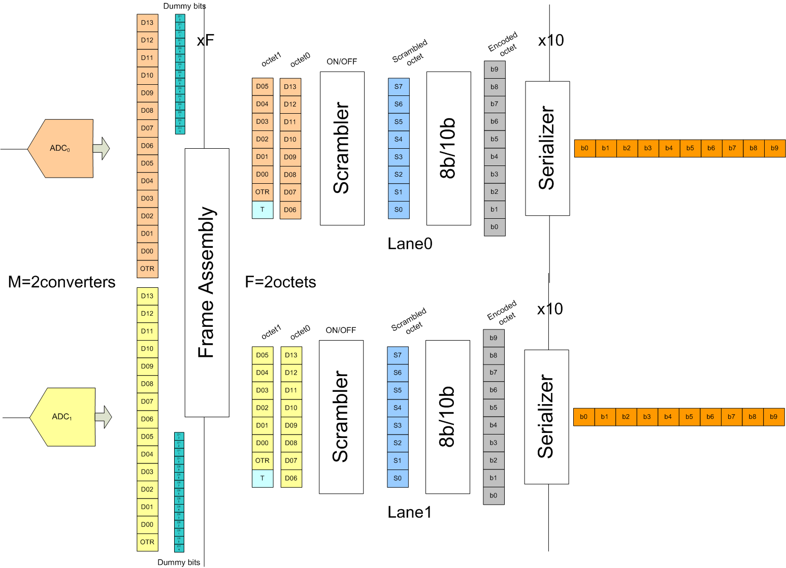
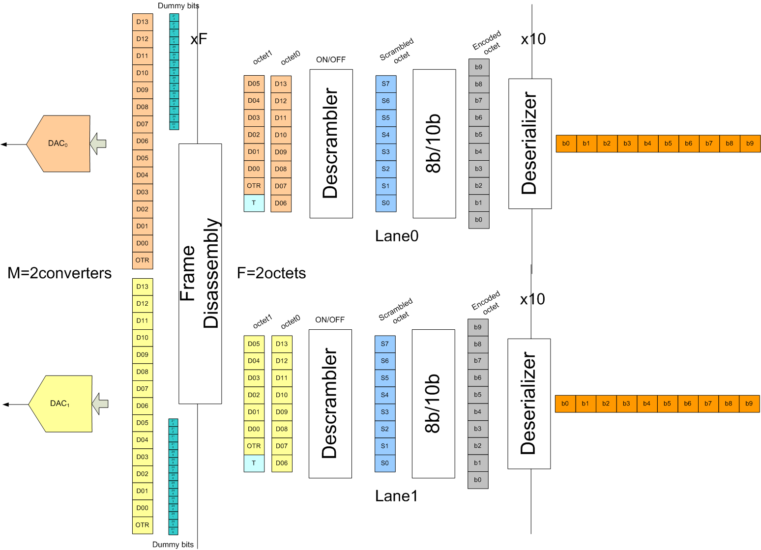
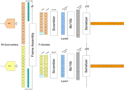 Figure 4 – Dual ADC Transmit Signal Chain
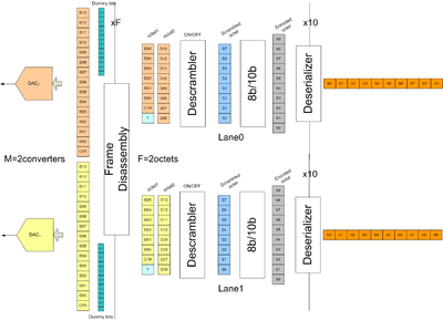 Figure 5 – Dual DAC Receive Signal Chain
There are several mapping options defined in the JESD204A specification:
- a single converter to a single-lane link
- multiple converters in the same device to a single-lane link
- a single converter to a multi-lane link
- and multiple converters in the same device to a multi-lane link
As mentioned above, the JESD204A standard also allows the system designer to combine multiple converter devices on a multi-point link. The JESD204A transport-layer framing-state machine groups samples and/or partial samples into frames of 8-bit octet data structures. The standard allows more than one sample per converter to be transmitted per frame cycle, with the constraint that the number of samples per converter per frame must be an integer, in order to minimize crosstalk between the SERDES digital circuits and the analog circuits.
In this specification, a sample is defined as N data bits plus optional control bits (such as over-range indication bits) plus optional tail bits. The tail bits are used at the end of the frame to fill out or pad out a whole number of octets per lane per frame cycle. Interestingly, the specification points out that constant value tail bits can cause spurious spectral lines if optional scrambling is not used. The use of pseudo-random tail bits is recommended. The specification also recommends the use of pseudo-random dummy bits during idle mode. The JESD204A transport layer maps samples to words (potentially adding control bits such as over-range indication) which are mapped to extended words (potentially adding tail bits to fill-out or pad-out 4-bit nibble groups, and, if necessary, adding tail bits to make the total number of bits a whole multiple of 8), which are mapped to 8-bit octets. The first user data octet transmitted in time corresponds to the most significant byte; the second user data octet transmitted in time corresponds to the least significant byte. Figure 4 illustrates the basic dual ADC transmit signal chain, and Figure 5 illustrates the basic dual DAC receive signal chain.
JESD204A Data Framing
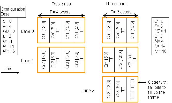
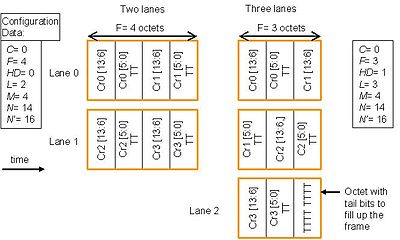 Figure 6 – Example of multi-lane user data format: four 14-bit converters over two or three lanes
In this specification, a frame data structure is a set of consecutive octets (an octet is the input to an 8B/10B encoder or the output from an 8B/10B decoder) in which the position of each octet is referenced to the frame alignment signal. A multiframe data structure is a set of consecutive frames in which the position of each frame is referenced to a multiframe alignment signal (generally a divided-down version of the frame alignment signal, just as the multiframe clock is a generally divided-down version of the frame clock). JESD204A defines three key parameters (see Figure 1):
- L is the lanes per link (or per converter device)
- M is the data converters per device/package
- F is the bytes (octets) per frame clock period.
The specification also defines CF to be the number of control words per frame clock period per link, and CS to be the number of control bits per conversion sample. K defines the number of frames per multiframe, N defines the converter resolution, N' defines the total number of bits per sample (quantized to 4-bit nibbles), HD defines the density mode (0: low density; 1: high density), and S defines the number of samples transmitted per single converter per frame (i.e., the oversampling ratio). The table below summarizes these parameters, and figure 6 illustrates a generic example of data framing format.
Abbreviation Designation M Data converters per device L Lanes per converter device F Octets per frame clock cycle CF Control words per frame clock cycle and link CS Number of control bits per conversion sample K Frames per multi-frame N Converter resolution (bits) N' Total bits per sample (incl. over-range bits) HD Density mode (0: low density; 1: high density) S Samples transmitted per single converter and frame clock cycle (i.e., oversampling ratio) The JESD204A Interface Modes
The JESD204A interface can work in one of the following modes:
- Fundamental mode vs. oversampled mode
- Fundamental mode vs. interpolating or decimating mode
- Data mode vs. test mode
- Active mode vs. idle mode
In the fundamental mode/data mode/active mode, one sample is transmitted per frame clock cycle from each transmitter (ADC or logic device) over the data lane to the receiver (DAC or logic device).
Oversampling ADCs typically provide decimation digital filtering to reduce the output sample rate to a more easily managed frequency. In the JESD204A standard, the distinction between non-decimating ADCs and decimating ADCs is minor: it introduces an additional clock domain in the frame assembly logic of the transmitter. In a non-decimating ADC, the sample clock is the frame clock. In a decimating ADC, the decimation clock is the frame clock (sample rate = frame rate x decimation factor). In oversampling ADCs without decimation, all samples are actually transmitted over the serial data lane (decimation factor = 1).
Likewise, interpolating DACs introduce an additional clock domain in the frame dis-assembly logic of the receiver. In this case: (output update rate = frame rate × interpolation factor). Clearly, the output update clock must be precise and low jitter. JESD204A supports oversampled DACs without interpolation, in which case, all samples are actually transmitted over the serial data lane (interpolation factor = 1). If used in conjunction with oversampling, it is important that the decimation factor and/or interpolation factor are chosen carefully by the system engineer to avoid the generation of unwanted analog spectral spurs.
Test modes can be implemented at the data link layer (e.g., by transmitting a stream of synchronization control characters) or at the transport layer, by transmitting a stream of test samples.
In idle mode, one or more converters in a device may be shut down / powered-down and the link kept active and synchronized. In idle mode, samples of inactive converters are replaced by dummy samples. At the data link layer, no difference can be seen between an active and an inactive (idle mode) converter. The presence of dummy samples is indicated to the receiver via the control interface or via dedicated (proprietary) control bits in the sample stream.
JESD204A allows for link power-down (shut-down mode), for power savings when the application is inactive or in standby. Operation in shut-down mode is similar to the fundamental mode, but with power-down and power-up procedures applied between the periods of activity. These power-down and power-up procedures are not part of the current JESD204A specification and their implementation is left to the application layer. Link resynchronization is required when transitioning back to full operating mode.
Optional JESD204A Data Scrambling and Test Mode
JESD204A also includes optional data scrambling prior to 8B/10B encoding, to de-correlate repeated data patterns and help to avoid related spurious tones induced in the analog domain. The defined scrambler is based on the polynomial 1 + x14 + x15, with a period of 32,767 bits. It is self-synchronous, allowing the descrambler to synchronize in two octets. Data scrambling can help avoid unwanted spectral tones that can otherwise occur with high-speed serial transmission. The JESD204A specification includes a protocol definition for optional test modes and test samples. The transmitter transmits test sample sequences, and the receiver verifies the test sample sequence. NXP's JESD204A compliant data converters include Pseudo Random Bit Sequence (PRBS) generators at several stages in the JESD204A interface blocks. For examples, the transmit block includes three PRBS generators: one prior to frame assembly; one prior to scrambling and 8B/10B encoding; and one prior to the serializer. The PRBS generators are useful to the system engineer to facilitate testing of the serial interface and verifying the system bit error rate.
The JESD204A Data Link Layer
8B/10B Encoding
8B/10B encoding schemes date from the 1970s, and was patented by IBM in 1984 (that patent has now expired). It is used broadly in intra-board (chip-to-chip) and inter-board (backplane) serial communication protocols including PCI Express, serial ATA, gigabit Ethernet, XAUI and Serial RapidIO. Essentially, the use of 10 bits (1024 binary patterns known as symbols) to encode 8 bit octets (256 binary patterns) allows considerable flexibility in the choice of binary patterns to be used. Patterns with six or more consecutive equal bits (such as 01111 11000 or 11000 00011) are excluded (i.e., the valid 10B bit patterns are run-length limited), as are patterns in which the number of zeros and the number of ones differ by four or more (such as 11000 10000 or 11110 11100). Eliminating patterns of this type leads to the desired long-term DC balance in the signal, as well as to the desired self-clocking attribute (by virtue of the consistently high number of bit state transitions in the valid 10B bit patterns). The spare valid 10B bit patterns also allows for the definition of in-band control symbols. Several of these control symbols, also known as comma codes, comma characters, or comma symbols, are reserved for synchronization and alignment protocols.
System Synchronization and Alignment
For example, the K28.0 control symbol (denoted R) and the K28.3 control symbol (denoted A) are used by JESD204A for lane alignment, the K28.7 control symbol (denoted F) is used for frame alignment, the K28.5 control symbol (denoted K) is used for user data code group synchronization. These control symbols and their two valid code groups are shown in the table below. Running Disparity is denoted RD.
Input Input RD = −1 RD = +1 Symbol HGF EDCBA abcdei fghj abcdei fghj Abbreviation K28.0 000 11100 001111 0100 110000 1011 R K28.3 011 11100 001111 0011 110000 1100 A K28.4 100 11100 001111 0010 110000 1101 Q K28.5 101 11100 001111 1010 110000 0101 K K28.7 111 11100 001111 1000 110000 0111 F 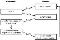 Figure 7 – Code Group Synchronization Sequence
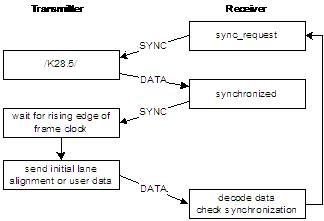
Among others, the JESD204A specification defines the essential code group user data synchronization protocol sequence.
At system reset (or subsequently, should user data synchronization be lost), the receivers assert SYNC~, causing multiple K28.5 control symbols to be sent from the transmitters (ADCs, FPGA, or ASIC). Once four valid K28.5 control symbols are received, the receivers de-assert the SYNC~ signal. The transmitters then send valid 10B user data symbols at the beginning of the next frame. This sequence can be illustrated as shown in figure 7.
In systems with multiple lanes, the SYNC~ signals from all receivers (DACs or FPGA) are combined and asserted simultaneously to all transmitters (ADCs or FPGA). As long as a single receiver requests synchronization, all transmitters attached to the link or the multipoint link will send K28.5 control symbols during initial code group synchronization. Of course, synchronization resolution is limited by the skew budget in the system.
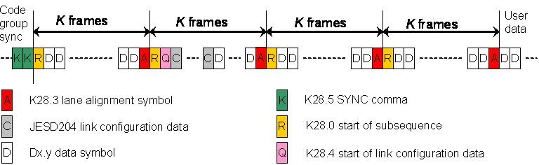
Lane Alignment
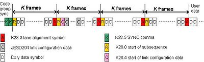 Figure 8 – Initial Lane Alignment Sequence with Four Multiframes
In JESD204A, the lane alignment protocol occurs immediately after the code group user data symbol synchronization protocol described above. In this protocol sequence, the K28.0 control symbol signals the receiver that lane alignment is underway. The K28.4 control signal (denoted Q) indicates the start of link configuration data. The K28.3 control symbol marks the end of the multiframe. This protocol sequence is shown in Figure 8.
The synchronization/alignment schemes defined by JESD204A are quite clever. For example, in the frame alignment monitoring protocol, 8B/10B user data symbols are themselves used as periodic frame alignment symbols (a technique called character replacement), enabling frame alignment without data loss. There are two modes of this protocol, both of which use the K28.7 and the K28.3 control symbols. In the case when scrambling is disabled, the transmitter examines the last octet in the current frame, and if it equals the last octet in the previous frame, the transmitter replaces that octet with a K28.7 frame alignment control symbol (in multiframe situations, the transmitter replaces that octet with a K28.3 frame alignment control symbol). Upon detecting a K28.7 or a K28.3 control symbol, the receiver replaces it with the value of the octet decoded at the end of the previous frame. In the case when scrambling is enabled, the transmitter examines the last octet in the current frame, and if it equals 0xFC, the transmitter replaces that octet with a K28.7 frame alignment control symbol. If the last octet in the current frame equal 0x7C, the transmitter replaces that octet with a K28.3 frame alignment control symbol. Upon detecting a K28.7 or K28.3 control symbol, the receiver replaces it with 0xFC or 0x7C, respectively. Note that the scrambler should naturally generate a frame alignment control symbol on average once every 256 frames. In both cases (with scrambling disabled and with scrambling enabled), if the receiver detects two successive valid frame alignment control symbols (K28.7 or K28.3) at the same position, but not at the end of the their associated frames, the receiver re-aligns it frame to the position indicated by the frame alignment control symbols. Note that this periodic frame alignment monitoring protocol is optional, because certain conversion signals (such as noise-free periodic signals possessing a harmonic relationship to the sample clock frequency) may not generate frame alignment control symbols when scrambling is disabled; generally this problem can be overcome with a small amount of dither. Designers/implementers should refer to the JEDEC JESD204A specification for complete details on these synchronization and alignment protocols.
JESD204A Scalability and Performance
It is straight forward to calculate the number of JESD204A links required to support an ADC or DAC, based on the converter resolution and the desired sampling rate. For a first example, consider a single-channel 12-bit non-oversampled ADC with one over-range bit per sample. Obviously, 13 bits are required per sample (N = 12 plus OTR over-range bit). As should be clear from the information in this article, JESD204A quantizes data and control information sent over the link to 8-bit octets (N' = 16). For a single-channel ADC with N' = 16, it should be clear that two octets are needed, with the unused three bits padded out with tail bits. After the 8B/10B encoder, each octet expands to 10 bits. With the link frequency at 3.125 Gbit/s, the maximum sample frequency is (3.125 Gbps / 20 bits per dual samples) = 156.25 MS/s per link.
For a second example, consider a dual-channel 14-bit non-oversampling DAC (such as the NXP Semiconductors DAC1408D650); note that this DAC includes four JESD204A receivers. In this case, N = 14, N' = 16, and four octets are required for the two channels, padded with four tail bits. With the link frequency at 3.125 Gbit/s, the maximum sample frequency is (3.125 Gbps / 40 bits per dual samples) = 78.125 MSPS per link. Four links support 312.5 MSPS maximum. NXP has found that the JEDEC JESD204A interface has little or no impact on analog performance. For example, the NXP ADC1413D125 achieves better than 85 dBc of SFDR performance typically, while consuming 1140 mW typically.
Conclusion
The new JEDEC JESD204A data converter interface definition has numerous system-level technical merits:
- Simplified PCB layout and routing
- Data converter and FPGA or ASIC pin count reduction
- Reduced signal skew management
- No PCB redesign for data converter resolution changes (10 to 16-bit), only FPGA logic reconfiguration
- Single bit error detect, by virtue of the computed running parity applied to the 8B/10B symbols
- Four or more time-aligned and phase coherent data converter channels for system designs such as LTE MIMO base stations
- Interoperability with Altera, Lattice and Xilinx FPGAs
- Periodic frame alignment monitoring and character replacement with the potential to maintain frame alignment without data loss
- Optional data and control symbol scrambling to produce data independence across the JESD204A link, with the potential to reduce non-harmonic spurs in the data converter analog domain
See also
External links
- NXP First JESD204A products available on the market, NXP Semiconductors
- NXP JESD204A CGVTM, Fast track your design, NXP Semiconductors
- Explanation of the trademarked acronym "CGV" (Convertisseur Grande Vitesse) - a proprietary superset of JESD204A
- Application note Xilinx Virtex-5 FPGA Interface to a JESD204A Compliant ADC, Xilinx
- JESD204A IP Core User’s Guide, Lattice Semiconductor
- Application note Interconnection between JESD204A compliant devices, NXP Semiconductors
- Application note JESD204A: New serialization technique for high speed data converters, NXP Semiconductors
References
Categories:
Wikimedia Foundation. 2010.