- Voltage doubler
-
A voltage doubler is an electronic circuit which charges capacitors from the input voltage and switches these charges in such a way that, in the ideal case, exactly twice the voltage is produced at the output as at its input.
The simplest of these circuits are a form of rectifier which take an AC voltage as input and output a doubled DC voltage. The switching elements are simple diodes and they are driven to switch state merely by the alternating voltage of the input. DC to DC voltage doublers cannot switch in this way and require a driving circuit to control the switching. They frequently also require a switching element that can be controlled directly, such as a transistor, rather than relying on the voltage across the switch as in the simple AC to DC case.
Voltage doublers are a variety of voltage multiplier circuit. Many (but not all) voltage doubler circuits can be viewed as a single stage of a higher order multiplier: cascading identical stages together achieves a greater voltage multiplication.
Contents
Voltage doubling rectifiers
Villard circuit
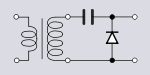 Figure 1. Villard circuit
The Villard circuit consists simply of a capacitor and a diode. While it has the great benefit of simplicity, its output has very poor ripple characteristics. Essentially, the circuit is a diode clamp circuit. The capacitor is charged on the negative half cycles to the peak AC voltage (Vpk). The output is the superposition of the input AC waveform and the steady DC of the capacitor. The effect of the circuit is to shift the DC value of the waveform. The negative peaks of the AC waveform are "clamped" to 0 V (actually −VF, the small forward bias voltage of the diode) by the diode, therefore the positive peaks of the output waveform are 2Vpk. The peak-to-peak ripple is an enormous 2Vpk and cannot be smoothed unless the circuit is effectively turned into one of the more sophisticated forms.[1]
Greinacher circuit
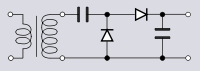 Figure 2. Greinacher circuit
The Greinacher voltage doubler is a significant improvement over the Villard circuit for a small cost in additional components. The ripple is much reduced, nominally zero under open-circuit load conditions, but when current is being drawn depends on the resistance of the load and the value of the capacitors used. The circuit works by following a Villard cell stage with what is in essence a peak detector or envelope detector stage. The peak detector cell has the effect of removing most of the ripple while preserving the peak voltage in the output.
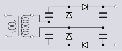 Figure 3. Voltage quadrupler – two Greinacher cells of opposite polarities
This circuit was first invented by Heinrich Greinacher in 1913 (published 1914[2]) to provide the 200–300 V he needed for his newly invented ionometer, the 110 V AC supplied by the Zurich power stations of the time being insufficient.[3] He later (1920) extended this idea into a cascade of multipliers.[4] This cascade of Greinacher cells is often inaccurately referred to as a Villard cascade. It is also called a Cockcroft–Walton multiplier after the particle accelerator machine built by John Cockcroft and Ernest Walton, who independently rediscovered the circuit in 1932.[5]
The concept in this topology can be extended to a voltage quadrupler circuit by using two Greinacher cells of opposite polarities driven from the same AC source. The output is taken across the two individual outputs. As with a bridge circuit, it is impossible to simultaneously ground the input and output of this circuit.[6]
Bridge circuit
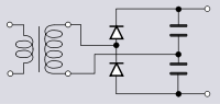 Figure 4. Bridge (Delon) voltage doubler
The Delon circuit uses a bridge topology for voltage doubling. This form of circuit was, at one time, commonly found in cathode ray tube television sets where it was used to provide an e.h.t. voltage supply. Generating voltages in excess of 5 kV with a transformer has safety issues in terms of domestic equipment and in any case is uneconomic. However, black and white television sets required an e.h.t. of 10 kV and colour sets even more. Voltage doublers were used to either double the voltage on an e.h.t winding on the mains transformer or were applied to the waveform on the line flyback coils.[7]
The circuit consists of two half-wave peak detectors, functioning in exactly the same way as the peak detector cell in the Greinacher circuit. Each of the two peak detector cells operates on opposite half-cycles of the incoming waveform. Since their outputs are in series, the output is twice the peak input voltage.
Switched capacitor circuits
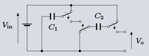 Figure 5. Switched capacitor voltage doubler achieved by simply switching charged capacitors from parallel to series
It is possible to use the simple diode-capacitor circuits described above to double the voltage of a DC source by preceding the voltage doubler with a chopper circuit. In effect, this converts the DC to AC before application to the voltage doubler.[8] More efficient circuits can be built by driving the switching devices from an external clock so that both functions, the chopping and multiplying, are achieved simultaneously. Such circuits are known as switched capacitor circuits. This approach is especially useful in low-voltage battery-powered applications where integrated circuits require a voltage supply greater than the battery can deliver. Frequently, a clock signal is readily available on-board the integrated circuit and little or no additional circuitry is needed to generate it.[9]
Conceptually, perhaps the simplest switched capacitor configuration is that shown schematically in figure 5. Here two capacitors are simultaneously charged to the same voltage in parallel. The supply is then switched off and the capacitors are switched into series. The output is taken from across the two capacitors in series resulting in an output double the supply voltage. There are many different switching devices that could be used in such a circuit, but in integrated circuits MOSFET devices are frequently employed.[10]
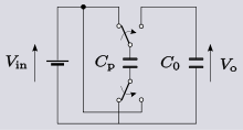 Figure 6. Charge-pump voltage doubler schematic
Another basic concept is the charge pump, a version of which is shown schematically in figure 6. The charge pump capacitor, CP, is first charged to the input voltage. It is then switched to charging the output capacitor, CO, in series with the input voltage resulting in CO eventually being charged to twice the input voltage. It may take several cycles before the charge pump succeeds in fully charging C2 but after steady state has been reached it is only necessary for CP to pump a small amount of charge equivalent to that being supplied to the load from CO. While CO is disconnected from the charge pump it partially discharges into the load resulting in ripple on the output voltage. This ripple is smaller for higher clock frequencies since the discharge time is shorter, and is also easier to filter. Alternatively, the capacitors can be made smaller for a given ripple specification. The practical maximum clock frequency in integrated circuits is typically in the hundreds of kHz.[11]
Dickson charge pump
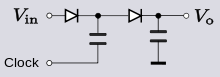 Figure 7. Dickson charge-pump voltage-doubler
The Dickson charge pump, or Dickson multiplier, consists of a cascade of diode/capacitor cells with the bottom plate of each capacitor driven by a clock pulse train. The circuit is a modification of the Cockcroft-Walton multiplier but takes a DC input with the clock trains providing the switching signal instead of the an AC input. The Dickson multiplier normally requires that alternate cells are driven from clock pulses of opposite phase. However, since a voltage doubler, shown in figure 7, requires only one stage of multiplication only one clock signal is required.[12]
The Dickson multiplier is frequently employed in integrated circuits where the supply voltage (from a battery for instance) is lower than that required by the circuitry. It is advantageous in integrated circuit manufacture that all the semiconductor components are of basically the same type. MOSFETs are commonly the standard logic block in many integrated circuits. For this reason the diodes are often replaced by this type of transistor, but wired to function as a diode - an arrangement called a diode-wired MOSFET. Figure 8 shows a Dickson voltage doubler using diode-wired n-channel enhancement type MOSFETs.[13]
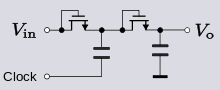 Figure 8. Dickson voltage doubler using diode-wired MOSFETs
There are many variations and improvements to the basic Dickson charge pump. Many of these are concerned with reducing the effect of the transistor drain-source voltage. This can be very significant if the input voltage is small, such as a low-voltage battery. With ideal switching elements the output is an integral multiple of the input (two for a doubler) but with a single-cell battery as the input source and MOSFET switches the output will be far less than this value since much of the voltage will be dropped across the transistors. For a circuit using discrete components the Schottky diode would be a better choice of switching element for its extremely low voltage drop in the on state. However, integrated circuit designers prefer to use the easily available MOSFET and compensate for its inadequacies with increased circuit complexity.[14]
As an example, an alkaline battery cell has a nominal voltage of 1.5 V. A voltage doubler using ideal switching elements with zero voltage drop will output double this, namely 3.0 V. However the drain-source voltage drop of a diode-wired MOSFET when it is in the on state must be at least the gate threshold voltage which might typically be 0.9 V.[15] This voltage "doubler" will only succeed in raising the output voltage by about 0.6 V to 2.1 V. If the drop across the final smoothing transistor is also taken into account the circuit may not be able to increase the voltage at all without using multiple stages. A typical Schottky diode, on the other hand, might have an on state voltage of 0.3 V.[16] A doubler using this Schottky diode will result in a voltage of 2.7 V at the output.[17]
Cross-coupled switched capacitors
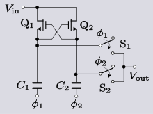 Figure 9. Cross-coupled switched-capacitor voltage doubler
Cross-coupled switched capacitor circuits come into their own for very low input voltages. Wireless battery driven equipment (pagers, bluetooth devices and the like) may require a single-cell battery to continue to supply power when it has discharged to under a volt.[18]
When clock
 is low transistor Q2 is turned off. At the same time clock
  is high turning on transistor Q1 resulting in capacitor C1 being charged to Vin. When goes high the top plate of C1 is pushed up to twice Vin. At the same time switch S1 closes so this voltage appears at the output. At the same time Q2 is turned on allowing C2 to charge. On the next half cycle the roles will be reversed: will be low, will be high, S1 will open and S2 will close. Thus, the output is supplied with 2Vin alternately from each side of the circuit.[19]
The loss is low in this circuit because there are no diode-wired MOSFETs and their associated threshold voltage problems. The circuit also has the advantage that the ripple frequency is doubled because there are effectively two voltage doublers both supplying the output from out of phase clocks. The primary disadvantage of this circuit is that stray capacitances are much more significant than with the Dickson multiplier and account for the larger part of the losses in this circuit.[20]
See also
- Voltage tripler
- DC to DC converter
- Flyback converter
- Boost converter
- Buck-boost converter
References
- ^ Kind and Feser, p. 28
- ^ Greinacher, H, "The Ionometer and its Application to the Measurement of Radium and Röntgen Rays", Physikal. Zeitsch., vol 15, 1914, pp. 410–415.
- ^ Mehra, p. 284
- ^ Kind and Feser, p. 29
- ^ Kind and Feser, p. 30
- ^ Ryder, p. 107
- ^ Kories and Schmidt-Walter, p.615
Millman and Halkias, p. 109
Wharton and Howorth, pp. 68–69 - ^ McComb, pp.148-150
- ^ Liu, pp.225-226
- ^ Ahmed, p.164
- ^ Zumbahlen, p.741
- ^ Liu, p.226
Yuan, pp.13-14 - ^ Liu, p.226
Yuan, p.14 - ^ Liu, pp.228-232
Yuan, 14-21 - ^ Liou et al., p.185
- ^ Bassett and Taylor, p.17/27
- ^ Yuan, p.17
- ^ Peluso et al., pp.36-37
Liu, pp.232-234 - ^ Campardo et al., p.377
Peluso et al., p.36
Liu, p.234 - ^ Peluso et al., p.36
Liu, p.234
Bibliography
- Ahmed, Syed Imran Pipelined ADC Design and Enhancement Techniques, Springer, 2010 ISBN 904818651X.
- Bassett, R.J.; Taylor, P.D., "17. Power Semiconductor Devices", Electrical Engineer's Reference Book, pp.17/1-17/37, Newnes, 2003 ISBN 0750646373.
- Campardo, Giovanni; Micheloni, Rino; Novosel, David VLSI-design of Non-volatile Memories, Springer, 2005 ISBN 354020198X.
- Kind, Dieter; Feser, Kurt High-voltage Test Techniques, translator Y. Narayana Rao, Newnes, 2001 ISBN 0750651830
- Kories, Ralf; Schmidt-Walter, Heinz Taschenbuch der Elektrotechnik: Grundlagen und Elektronik, Deutsch Harri GmbH, 2004 ISBN 3817117345.
- Liou, Juin J.; Ortiz-Conde, Adelmo; García-Sánchez, F. Analysis and Design of MOSFETs, Springer, 1998 ISBN 0412146010.
- Liu, Mingliang Demystifying Switched Capacitor Circuits, Newnes, 2006 ISBN 0750679077.
- McComb, Gordon Gordon McComb's gadgeteer's goldmine!, McGraw-Hill Professional, 1990 ISBN 083063360X.
- Mehra, J; Rechenberg, H The Historical Development of Quantum Theory, Springer, 2001 ISBN 0387951792.
- Millman, Jacob; Halkias, Christos C. Integrated Electronics, McGraw-Hill Kogakusha, 1972 ISBN 0070423156.
- Peluso, Vincenzo; Steyaert, Michiel; Sansen, Willy M. C. Design of Low-voltage Low-power CMOS Delta-Sigma A/D Converters, Springer, 1999 ISBN 0792384172.
- Ryder, J. D. Electronic Fundamentals & Applications, Pitman Publishing, 1970 ISBN 0273314912.
- Wharton, W.; Howorth, D. Principles of Television Reception, Pitman Publishing, 1971 ISBN 0273361031.
- Yuan, Fei CMOS Circuits for Passive Wireless Microsystems, Springer, 2010 ISBN 1441976795.
- Zumbahlen, Hank Linear Circuit Design Handbook, Newnes, 2008 ISBN 0750687037.
Categories:- Electrical circuits
- Electrical power conversion
- Analog circuits
- Electronics terms
- Electronic design


Wikimedia Foundation. 2010.