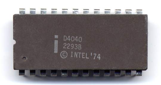
- Intel 4040
Infobox Computer Hardware Cpu
name = Intel 4040

caption = An Intel D4040 Microprocessor
produced-start = 1974
produced-end = 1981 [ [http://www.cpushack.net/life-cycle-of-cpu.html CPU History - The CPU Museum - Life Cycle of the CPU ] ]
slowest = 500 | slow-unit = kHz
fastest = 740 | fast-unit = kHz
fsb-slowest = | fsb-slow-unit =
fsb-fastest = | fsb-fast-unit =
manuf1 = Intel
arch =4-bit BCD oriented
pack1 = 24 pin DIPThe Intel 4040
microprocessor was the successor to theIntel 4004 . It was introduced in1974 . The 4040 employed a 10 μm silicon-gate enhancement load PMOS technology, was made up of 3,000transistor s [ [http://www.cpu-collection.de/?l0=co&l1=Intel&l2=4040 cpu-collection.de >> Intel >> 4040 ] ] and could execute approximately 60,000instructions per second .New features
*
Interrupt
*Single StepExtensions
*Instruction Set expanded to 60 instructions
*Program memory expanded to 8KB
*Registers expanded to 24
*Subroutine stack expanded to 7 levels deepDesigners
Federico Faggin proposed the project, formulated the architecture and led the design.The detailed design was done by Tom Innes.New support chips
*4201 - Clock Generator 500 to 740 kHz using 4 to 5.185 MHz crystals
*4308 - 1 KB ROM
*4207 - General Purpose byte Output port
*4209 - General Purpose byte Input port
*4211 - General Purpose byte I/O port
*4289 - Standard Memory Interface (replaces 4008/4009)
*4702 - 256 byte UVEPROM
*4316 - 2 KB ROM
*4101 - 256 4-bit word RAMReferences
Wikimedia Foundation. 2010.
