- Si/SiGe resonant interband tunnel diode
A Si/SiGe resonant interband tunnel diode (RITD) is a type of
resonant interband tunnel diode swhich is based on Si/SiGe materials.All types of tunnel diodes, including Si/SiGe resonant interband tunnel diodes,make use of the quantum mechanical tunneling effect.Characteristic to the current-voltage relationship of a tunnel diode is the presence ofone or more negative differential resistance region, which enables many unique applications.Tunnel diodes are also capable of high speed operation because the quantum tunneling effect is a fast process.
Compared to the Esaki
tunnel diode s, which are essentially discretediodes and therefore incompatible with modern Si integrated circuittechnologies, the Si/SiGe resonant interband tunnel diodes are such thattheir structure and fabrication are suitable for integration withmodern Si complemenraty metal-oxide-semiconductor (CMOS) and Si/SiGeheterojunction bipolar technology.Resonant tunnel diodes and
resonant interband tunnel diodeswere first realized in III-V compound materialsystems utilizing hetrojunctions made up of various III-V compoundsemiconductors.Reasonably high performance III-V resonant tunnel diodes have beenrealized. But such devices have not entered mainstream applications yetbecause the processing of III-V materials isincompatible with Si CMOS technology and the cost is high.Si/SiGe resonant tunnel diodessuffer from limited performance becauseof the limited conduction band and valance band offsets.
Si/SiGe resonant interband tunnel diodes are developed ref|Rommel98, which offerthe advantage of being compatible with the mainstream Si CMOS technology.
Structure
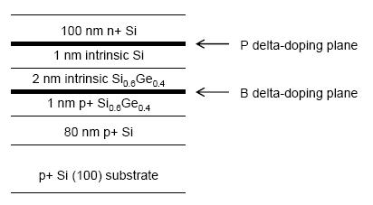
thumb|309px|right|Typical structure of a Si/SiGe resonant interbandtunnel diode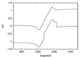
thumb|262px|right|Calculated band diagram of a typicalSi/SiGe resonant interband tunnel diodeThe structure of a typical Si/SiGe resonant interband tunnel didoe is shown on the right.Also shown is the corresponding band diagram calculated by [http://www.nd.edu/~gsnider/ Gregory Snider's 1D Poisson/Schrodinger Solver] .
The five key points to the design are:(i) an intrinsic tunneling barrier, (ii) delta-doped injectors, (iii) offset of the delta-doping planes from the
heterojunction interfaces,(iv) low temperature molecular beam epitaxial growth (LTMBE), and(v) postgrowth rapid thermal annealing (RTA) for dopant activation and point defect reductionref_label|Rommel98|1|a.Performance
A minimum PVCR of about 3 is needed for typical circuit applications.Low current density Si/SiGe RITDs are suitable for low-powermemory applications,and high current density tunndel diodes are needed for high speeddigital/mixed-signal applications.Si/SiGe RITDs have been engineered to have room temperature PCVRs upto 4.0 ref|Park2006.The same structure was duplicated by another research group usinga different MBE system, and PVCRs of up to 6.0have been obtainedref|Duschl2000.In terms of peak current density, peak current densities ranging from as low as 20 mA/cm2 and as high as 218 kA/cm2,spanning seven orders of magnitude, have been obtainedref|Chung06.A resistive cut-off frequency of 20.2 GHz has been realized onphotolithography defined SiGe RITD followedby wet etching for further reducing the diode size ref_label|Chung06|5|a,which shouldbe able to improve when even smaller RITDs are fabricated usingtechniques such as electron beam lithography.
Applications
In addition to the realization of integration with Si CMOS and SiGe HBT thatis discussed in the next section, other applications of SiGe RITD have beendemonstrated using breadboard circuits, including multi-state logic ref|Jin04.
Integration with Si/SiGe CMOS and HBTs
Integration of Si/SiGe RITDs with Si CMOS has been demonstrated ref|Sudirgo06.
Vertical integration of Si/SiGe RITD and SiGe HBT was also demonstrated,realizing a 3-terminal negative differential resistance circuit element withadjustable peak-to-valley current ratioref|Chung04.
These results indicate that Si/SiGe RITDs is a promising candidate of beingintegrated with the Si integrated circuit technology.
References
#note_label|l_Rommel98|9|a S.L. Rommel, T.E. Dillon, M.W. Dashiell, H. Feng, J. Kolodzey, P.R. Berger, P.E. Thompson, K.D. Hobart, R. Lake, A.C. Seabaugh, G. Klimeck, and D.K. Blanks, Room Temperature Operation of Epitaxially Grown Si/Si0.5Ge0.5/Si Resonant Interband Tunneling Diodes, Applied Physics Letters 73, 2191 (1998).
# S.-Y. Park, S.-Y. Chung, P.R. Berger, R. Yu, and P.E. Thompson, Low sidewall damage plasma etching using ICP-RIE with HBr chemistry of Si/SiGe resonant interband tunnel diodes, IEE Electronics Letters 42, 719 (2006).
# R. Duschl and K. Eberl, Physics and applications of Si/SiGe/Si resonant interband tunneling diodes, Thin Solid Films 380, 151 (2000).
# N. Jin, S.Y. Chung, R. Yu, R.M. Heyns, P.R. Berger, and P.E. Thompson, The effect of spacer thicknesses on Si-based resonant interband tunneling diode performance and their application to low-power tunneling diode SRAM circuits, IEEE Transactions on Electron Devices 53, 2243 (2006).
# S.Y. Chung, R. Yu, N. Jin, S.Y. Park, P.R. Berger, and P.E. Thompson, Si/SiGe Resonant Interband Tunnel Diode with fr0 20.2 GHz and Peak Current Density 218 kA/cm2 for K-band Mixed-Signal Applications, IEEE Electron Device Letters 27, 364 (2006).
# N. Jin, S.Y. Chung, R.M. Heyns, and P.R. Berger, R. Yu, P.E. Thompson, and S.L. Rommel, Tri-State Logic Using Vertically Integrated Si Resonant Interband Tunneling Diodes with Double NDR, IEEE Electron Device Letters 25, 646 (2004).
# S. Sudirgo, D.J. Pawlik, S.K. Kurinec, P.E. Thompson, J.W. Daulton, S.Y. Park, R. Yu, P.R. Berger, and S.L. Rommel, NMOS/SiGe Resonant Interband Tunneling Diode Static Random Access Memory, 64th Device Research Conference Conference Digest, page 265, June 26-28, 2006, The Pennsylvania State University, University Park, PA.
# S.Y. Chung, N. Jin, and P.R. Berger, R. Yu, P.E. Thompson, R. Lake, S.L. Rommel and S.K. Kurinec, 3-Terminal Si-Based Negative Differential Resistance Circuit Element with Adjustable Peak-To-Valley Current Ratios Using a Monolithic Vertical Integration, Applied Physics Letters 84, 2688-2690 (2004).External links
* [http://www.nd.edu/~gsnider/ Gregory Snider's 1D Poisson/Schrodinger Solver]
See also
*Si
Esaki tunnel diode
*Resonant tunnel diode
*Resonant interband tunnel diode
*Si/SiGe resonant tunnel diode
Wikimedia Foundation. 2010.